
Pcb design test

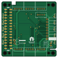
About the Pcb design test
Pcb design test is an open source PCB design by airpocket-soundman, published on GitHub. It is a 2-layer board measuring 50 × 50 mm, with 25 components from 10 distinct parts.
Other key parts include the SK6812SIDE-A. By type, the board carries 11 connectors, 10 ICs, 2 jumpers and 2 resistors.
From the project
pcbdesignをAId絵するテスト
M5Stackの上部本体(Core Basic)にとりつけて、以下のようなM5GO/Fireの機能やそれ以外の機能を追加できる底板(ベースボード)用の拡張基板です。 M5GOBaseLiteの後継機で、基本的な機能・回路は同一で、裏面のメスMbusコネクタが使えるようになりました。 - Groveコネクタ(PortA(2個), PortB, PortC, PortD, PortE)(PortA/B/CはM5Stack純正のものと同等です。PortD/EはM5Stack純正品にはありませんが、UI Flowで使用することができるポートです) - 左右5個ずつのNeoPixel (SK6812)(オプション) - LiPoバッテリ接続端子(オプション)
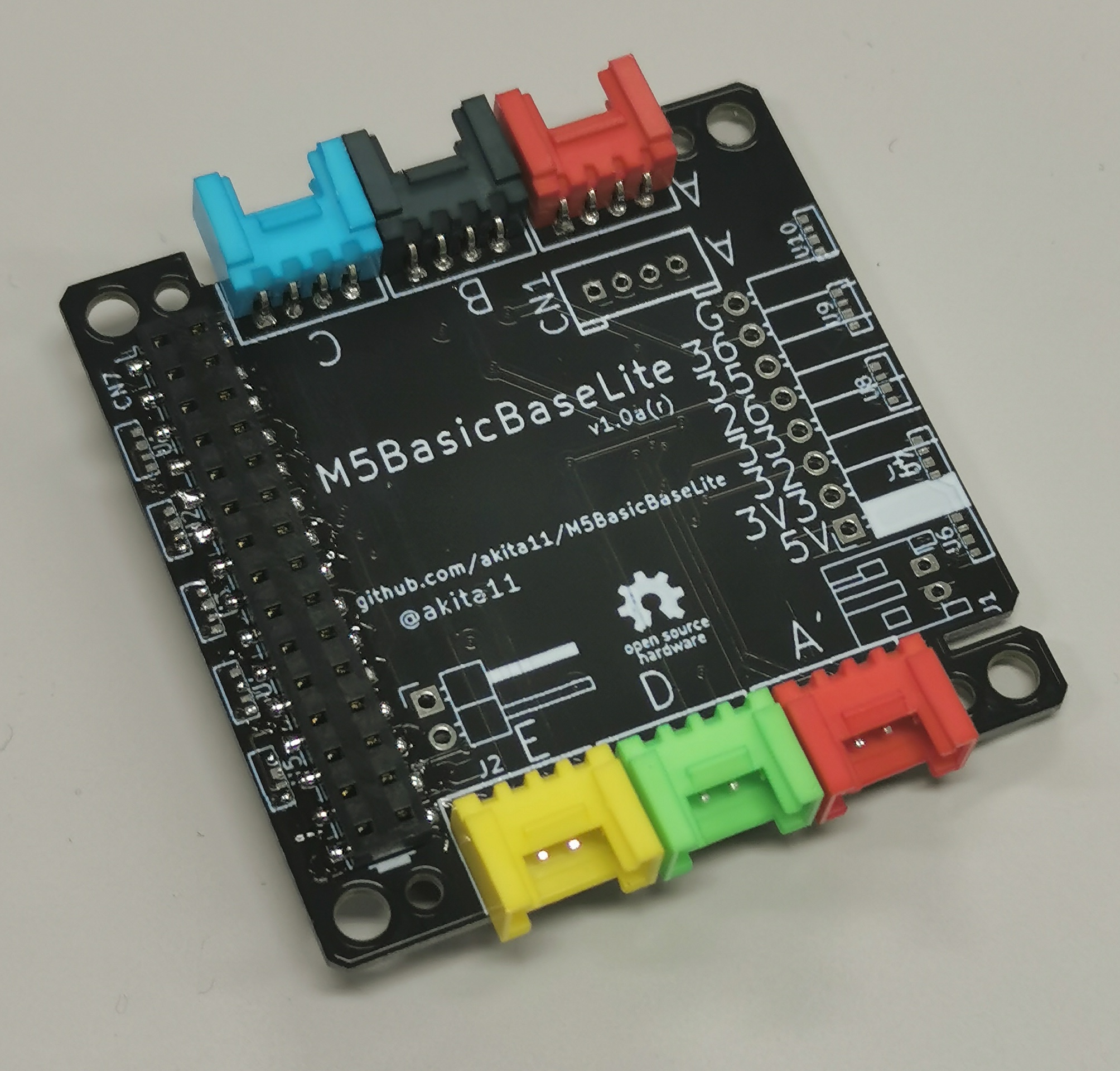
Main components on the Pcb design test
Pcb design test bill of materials (BOM)
25 components, 10 distinct parts — part numbers from the project's BOM.
| Qty | Part | Footprint | Refs |
|---|---|---|---|
| 10 | SK6812SIDE-A LED_SK6812side | LED_SK6812SIDE | U1, U2, U3, U4, U5, U6, U7, U8 +2 |
| 1 | CON_GROVEV | CON_GROVE_V | CN1 |
| 6 | CON_GROVEH | CON_GROVE_H | CN2, CN3, CN4, CN5, CN6, CN7 |
| 1 | MBUS_bottom | PinSocket_2x15_P2.54mm_Vertical_SMD | CN8 |
| 1 | Conn_01x02_Female | JST_PH_S2B-PH-K_1x02_P2.00mm_Horizontal | J1 |
| 1 | Conn_01x02_Female | PinHeader_1x02_P2.54mm_Horizontal | J2 |
| 1 | Conn_01x08_Female | PinSocket_1x08_P2.54mm_Horizontal | J3 |
| 1 | SolderJumper_2_Bridged | SolderJumper-2_P1.3mm_Bridged_Pad1.0x1.5mm | JP1 |
| 1 | SolderJumper_3_Bridged12 | SolderJumper-3_P1.3mm_Bridged2Bar12_Pad1.0x1.5mm | JP2 |
| 2 | 4.7k | 0603 | R1, R2 |
Pcb design test design files
The KiCad project lives in the airpocket-soundman/pcb_design_test repository on GitHub; these links point at the commit this page was built from.
Pcb design test: common questions
How big is the Pcb design test?
The Pcb design test measures 50 × 50 mm, has 2 copper layers and is 1.6 mm thick.
How many components are on the Pcb design test?
25 components, from 10 distinct parts, with part numbers taken from the project's own BOM. The full bill of materials is listed on this page.
Where can I download the Pcb design test design files?
From the airpocket-soundman/pcb_design_test repository on GitHub, which has the KiCad layout, the schematic and the BOM; the links under Design files point to each one.
Can I use the Pcb design test design in my own project?
The repository has no license, so all rights stay with airpocket-soundman. Use it as a reference, and ask the author before reusing the design.