CDE-3-debug

About the CDE-3-debug PCB
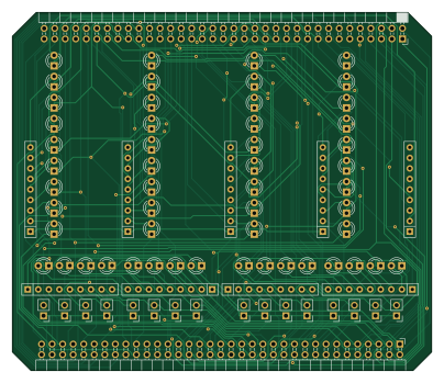
CDE-3-debug is an open source PCB design by ArqueologiaDigital, published on GitHub. It is a 2-layer board measuring 101 × 86.4 mm, with 79 components from 56 distinct parts.
By type, the board carries 52 diodes, 16 jumpers and 2 LEDs.
From the project
Schematics of the Patinho Feio CPU being redrawn on KiCAD. More info at: http://github.com/felipesanches/PatinhoFeio
Para o desenvolvimento desse projeto estou atualmente (Julho de 2025) utilizando o Kicad versão 9.0.2+dfsg-1 instalado a partir do repositório de pacotes do Debian 13. ----
Existe um arquivo patinhofeio.pro na raiz desse repo que referencia os demais sub-projetos de cada placa.
Em JAN/2018 eu encomendei a fabicação das PCBs CDE-3 e CDE-3-debug. Há um relato detalhado em https://forum.fiozera.com.br/t/resgate-historico-do-computador-patinho-feio-usp-1971/58/18
CDE-3-debug bill of materials (BOM)
79 components, 56 distinct parts.
| Qty | Part | Footprint | Refs |
|---|---|---|---|
| 16 | JUMPER | Pin_Header_Straight_1x02_Pitch2.54mm | JP1, JP2, JP3, JP4, JP5, JP6, JP7, JP8 +8 |
| 9 | RR8 | R_Array_SIP9 | RR1, RR2, RR3, RR4, RR5, RR6, RR7, RR8 +1 |
| 1 | CONN_35X2 | Socket_Strip_Angled_2x35_Pitch2.54mm | CONECTOR_FEMEA_DEBUG_CDE3 |
| 1 | CONN_35X2 | Pin_Header_Angled_2x35_Pitch2.54mm | CONECTOR_MACHO_DEBUG_CDE3 |
| 1 | +MICG1 | LED_D3.0mm | D1 |
| 1 | +MICG2A | LED_D3.0mm | D2 |
| 1 | +MICG2B | LED_D3.0mm | D3 |
| 1 | +IMEADD | LED_D3.0mm | D4 |
| 1 | +IMENAND | LED_D3.0mm | D5 |
| 1 | +IMEXOR | LED_D3.0mm | D6 |
| 1 | +SHIFT | LED_D3.0mm | D7 |
| 1 | +IME | LED_D3.0mm | D8 |
| 1 | RESERVADO | LED_D3.0mm | D9 |
| 1 | +INDICE | LED_D3.0mm | D10 |
| 1 | -RDZ | LED_D3.0mm | D11 |
| 1 | +SAEDS | LED_D3.0mm | D12 |
| 1 | +SAEDE | LED_D3.0mm | D13 |
| 1 | +SAESA | LED_D3.0mm | D14 |
| 1 | +SAEFU | LED_D3.0mm | D15 |
| 1 | +SAE | LED_D3.0mm | D16 |
Show 36 more
| Qty | Part | Footprint | Refs |
|---|---|---|---|
| 1 | +PLI | LED_D3.0mm | D17 |
| 1 | +ARA | LED_D3.0mm | D18 |
| 1 | +CAC | LED_D3.0mm | D19 |
| 1 | +SOM | LED_D3.0mm | D20 |
| 1 | +SUS | LED_D3.0mm | D21 |
| 1 | +PUG | LED_D3.0mm | D22 |
| 1 | +PAN | LED_D3.0mm | D23 |
| 1 | +PAZ | LED_D3.0mm | D24 |
| 1 | +MIC | LED_D3.0mm | D25 |
| 1 | +PUL | LED_D3.0mm | D26 |
| 1 | +TRO | LED_D3.0mm | D27 |
| 1 | +TRI | LED_D3.0mm | D28 |
| 1 | +INI | LED_D3.0mm | D29 |
| 1 | +PER | LED_D3.0mm | D30 |
| 1 | +ESP-D | LED_D3.0mm | D31 |
| 1 | +PAR-D | LED_D3.0mm | D32 |
| 1 | +(SUS+PUG) | LED_D3.0mm | D33 |
| 1 | +(PAN+PAZ) | LED_D3.0mm | D34 |
| 1 | +(CAC+SOM) | LED_D3.0mm | D35 |
| 1 | +(PLI+ARA) | LED_D3.0mm | D36 |
| 1 | +RD_0 | LED_D3.0mm | D37 |
| 1 | +RD_1 | LED_D3.0mm | D38 |
| 1 | +RD_2 | LED_D3.0mm | D39 |
| 1 | +RD_3 | LED_D3.0mm | D40 |
| 1 | +RD_4 | LED_D3.0mm | D41 |
| 1 | +RD_5 | LED_D3.0mm | D42 |
| 1 | +RD_6 | LED_D3.0mm | D43 |
| 1 | +RD_7 | LED_D3.0mm | D44 |
| 1 | +RI_0 | LED_D3.0mm | D45 |
| 1 | +RI_1 | LED_D3.0mm | D46 |
| 1 | +RI_2 | LED_D3.0mm | D47 |
| 1 | +RI_3 | LED_D3.0mm | D48 |
| 1 | +RI_4 | LED_D3.0mm | D49 |
| 1 | +RI_5 | LED_D3.0mm | D50 |
| 1 | +RI_6 | LED_D3.0mm | D51 |
| 1 | +RI_7 | LED_D3.0mm | D52 |
CDE-3-debug design files
The KiCad project lives in the ArqueologiaDigital/PatinhoFeio_KICAD repository on GitHub; these links point at the commit this page was built from.
CDE-3-debug: common questions
How big is the CDE-3-debug PCB?
The CDE-3-debug measures 101 × 86.4 mm, has 2 copper layers and is 1.6 mm thick.
How many components are on the CDE-3-debug?
79 components, from 56 distinct parts. The full bill of materials is listed on this page.
Where can I download the CDE-3-debug design files?
From the ArqueologiaDigital/PatinhoFeio_KICAD repository on GitHub, which has the KiCad layout and the schematic; the links under Design files point to each one.
Can I use the CDE-3-debug design in my own project?
The repository has no license, so all rights stay with ArqueologiaDigital. Use it as a reference, and ask the author before reusing the design.