
KiCad.Projects

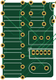
About the KiCad.Projects PCB
KiCad.Projects is an open source PCB design by BoBoBaSs84, published on GitHub under the MIT license. It is a 2-layer board measuring 19.3 × 28.4 mm, with 16 components from 9 distinct parts.
By type, the board carries 8 resistors, 3 capacitors, 2 connectors and 2 transformers.
From the project
All of my KiCad projects are stored here.
KiCad.Projects bill of materials (BOM)
16 components, 9 distinct parts.
| Qty | Part | Footprint | Refs |
|---|---|---|---|
| 1 | WAGO 734-135 | Wuerth_WR-WTB_64800511622_1x05_P1.50mm_Vertical | J1 |
| 1 | 100R | Potentiometer_Bourns_3296W_Vertical | P6 |
| 1 | 400kH | Resonator-2Pin_W8.0mm_H3.5mm | Qz2 |
| 2 | BC337 | TO-92 | T3, T4 |
| 3 | 1nF | C_Disc_D4.7mm_W2.5mm_P5.00mm | C4, C5, C6 |
| 1 | 33R | R_Axial_DIN0207_L6.3mm_D2.5mm_P7.62mm_Horizontal | R7 |
| 5 | 1k | R_Axial_DIN0207_L6.3mm_D2.5mm_P7.62mm_Horizontal | R8, R9, R10, R11, R12 |
| 1 | 2k7 | R_Axial_DIN0207_L6.3mm_D2.5mm_P7.62mm_Horizontal | R13 |
| 1 | 68R | R_Axial_DIN0207_L6.3mm_D2.5mm_P7.62mm_Horizontal | R14 |
KiCad.Projects design files
The KiCad project lives in the BoBoBaSs84/KiCad.Projects repository on GitHub; these links point at the commit this page was built from.
KiCad.Projects: common questions
How big is the KiCad.Projects PCB?
The KiCad.Projects measures 19.3 × 28.4 mm, has 2 copper layers and is 1.6 mm thick.
How many components are on the KiCad.Projects?
16 components, from 9 distinct parts. The full bill of materials is listed on this page.
Where can I download the KiCad.Projects design files?
From the BoBoBaSs84/KiCad.Projects repository on GitHub, which has the KiCad layout and the schematic; the links under Design files point to each one.
Can I use the KiCad.Projects design in my own project?
Yes, under the terms of its MIT license, which BoBoBaSs84 chose for the repository.