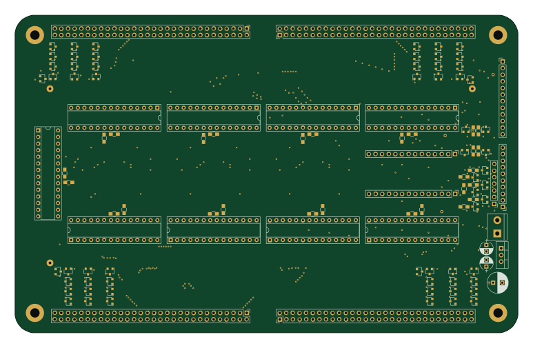
LED Daughterboard

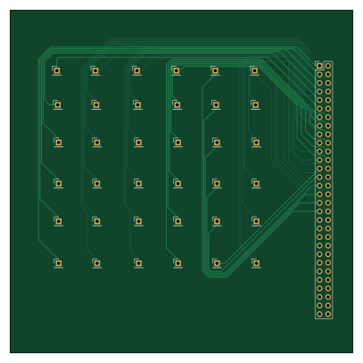
About the LED Daughterboard PCB
LED Daughterboard is an open source PCB design by c3n3, published on GitHub. It is a 2-layer board measuring 101.6 × 101.6 mm, with 37 components from 2 distinct parts.
From the project
LED^3
Hello person who wishes to learn the cube's ways! This will be a BRIEF introduction... Basically the situation is as follows: we have a cube, it is a 12 x 12 x 12 cube of RGB LEDs, we have this newly (but probably old when your reading this) created softare architecture that will hopefully stand the test of time (you decide). The things you want to look into are:
LED Daughterboard bill of materials (BOM)
37 components, 2 distinct parts.
| Qty | Part | Footprint | Refs |
|---|---|---|---|
| 1 | Conn_02x30_Top_Bottom | Pin_Header_Straight_2x30_Pitch2.54mm | P7 |
| 36 | Conn_01x01 | Pin_Header_Straight_1x01_Pitch2.54mm | (0,0)1, (0,1)1, (0,2)1, (0,3)1, (0,4)1, (0,5)1, (1,0)1, (1,1)1 +28 |
LED Daughterboard design files
The KiCad project lives in the c3n3/LEDCubed repository on GitHub; these links point at the commit this page was built from.
LED Daughterboard: common questions
How big is the LED Daughterboard PCB?
The LED Daughterboard measures 101.6 × 101.6 mm, has 2 copper layers and is 1.6 mm thick.
How many components are on the LED Daughterboard?
37 components, from 2 distinct parts. The full bill of materials is listed on this page.
Where can I download the LED Daughterboard design files?
From the c3n3/LEDCubed repository on GitHub, which has the KiCad layout; the links under Design files point to each one.
Can I use the LED Daughterboard design in my own project?
The repository has no license, so all rights stay with c3n3. Use it as a reference, and ask the author before reusing the design.