
Main

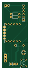
About the Main PCB
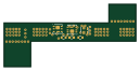
Main is an open source PCB design by cho45, published on GitHub. It is a 2-layer board measuring 24 × 59 mm, with 14 components from 8 distinct parts.
Other key parts include the BLE_NANO. By type, the board carries 3 resistors, 1 IC, 1 connector, 1 battery holder, 1 switch and 1 diode.
It belongs with the keyboards designs in this gallery.
From the project
Keyboard project
Open Root.sch for viewing overall schematic.
BLE Nano (nRF51288) MCP23017 (I2C GPIO) * Gateron Switches (Cherry MX compatible)
https://developer.mbed.org/users/cho45/code/keyboard/
Main components on the Main
Main bill of materials (BOM)
14 components, 8 distinct parts.
| Qty | Part | Footprint | Refs |
|---|---|---|---|
| 1 | BLE_NANO | BLE_NANO | U3 |
| 1 | CONN_01X06 | Pin_Header_Straight_1x06 | P1 |
| 1 | Battery | Pin_Header_Straight_1x02 | BT1 |
| 6 | CONN_01X01 | Socket_Strip_Straight_1x01 | P_GND1, P_GND2, P_RXD1, P_SWCLK1, P_SWDIO1, P_TXD1 |
| 1 | SW_RESET | SW_TH_Tactile_Omron_B3F-10xx | SW1 |
| 1 | LED | LED-3MM | D1 |
| 1 | 4.7k | Resistor_Horizontal_RM7mm | R1 |
| 2 | 10k | Resistor_Horizontal_RM7mm | R2, R3 |
Main design files
The KiCad project lives in the cho45/Keble repository on GitHub; these links point at the commit this page was built from.
- LayoutMain.kicad_pcb
Main: common questions
How big is the Main PCB?
The Main measures 24 × 59 mm, has 2 copper layers and is 1.6 mm thick.
How many components are on the Main?
14 components, from 8 distinct parts. The full bill of materials is listed on this page.
Where can I download the Main design files?
From the cho45/Keble repository on GitHub, which has the KiCad layout; the links under Design files point to each one.
Can I use the Main design in my own project?
The repository has no license, so all rights stay with cho45. Use it as a reference, and ask the author before reusing the design.
 byrantech

 google