
Kindle adapter

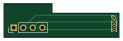
About the Kindle adapter PCB
Kindle adapter is an open source PCB design by edoput, published on GitHub. It is a 2-layer board measuring 30.5 × 8.9 mm, with 2 components from 2 distinct parts.
From the project
easy connect to your kindle serial debug port
A physical adapter going from a 1.8V serial USB converter to the kindle UART debugging pads
The kindle UART debugging pads are tiny and very close, by (not so) careful measurement I think they are spaced as a 0.1mm header, we'll see about that.
Also the on board circuitry runs at 1.8V so you need an serial USB adapter already running at 1.8V to keep the magic smoke inside.
Kindle adapter bill of materials (BOM)
2 components, 2 distinct parts.
| Qty | Part | Footprint | Refs |
|---|---|---|---|
| 1 | Conn_01x04 | PinHeader_1x04_P2.54mm_Vertical | J1 |
| 1 | Conn_01x04 | PinHeader_1x04_P1.00mm_Vertical | J2 |
Kindle adapter design files
The KiCad project lives in the edoput/kindle-adapter repository on GitHub; these links point at the commit this page was built from.
- Layoutkindle-adapter.kicad_pcb
Kindle adapter: common questions
How big is the Kindle adapter PCB?
The Kindle adapter measures 30.5 × 8.9 mm, has 2 copper layers and is 1.6 mm thick.
How many components are on the Kindle adapter?
2 components, from 2 distinct parts. The full bill of materials is listed on this page.
Where can I download the Kindle adapter design files?
From the edoput/kindle-adapter repository on GitHub, which has the KiCad layout; the links under Design files point to each one.
Can I use the Kindle adapter design in my own project?
The repository has no license, so all rights stay with edoput. Use it as a reference, and ask the author before reusing the design.