
Kill LIFE

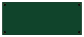
About the Kill LIFE PCB
Kill LIFE is an open source PCB design by electron-rare, published on GitHub under the MIT license. It is a 2-layer board measuring 68.6 × 27.9 mm, with 4 components from 1 distinct parts.
From the project
Kill_LIFE — spec-first agentic methodology for embedded systems (ESP32/STM32, gates, evidence packs, BMAD agents)
- kicad/ : projets KiCad - rules/ : règles champs/footprints/nets - blocks/ : Design Blocks KiCad 10 (bibliothèque de briques)
⚠️ Les fichiers KiCad réels sont à créer/committer depuis ton poste. Ce template fournit l’outillage (schops + gates + CI).
Kill LIFE bill of materials (BOM)
4 components, 1 distinct parts — part numbers from the project's BOM.
| Qty | Part | Footprint | Refs |
|---|---|---|---|
| 4 | — | MH_2_2, MH_2_26, MH_67_2, MH_67_26 |
Kill LIFE design files
The KiCad project lives in the electron-rare/Kill_LIFE repository on GitHub; these links point at the commit this page was built from.
Kill LIFE: common questions
How big is the Kill LIFE PCB?
The Kill LIFE measures 68.6 × 27.9 mm, has 2 copper layers and is 1.6 mm thick.
How many components are on the Kill LIFE?
4 components, from 1 distinct parts, with part numbers taken from the project's own BOM. The full bill of materials is listed on this page.
Where can I download the Kill LIFE design files?
From the electron-rare/Kill_LIFE repository on GitHub, which has the KiCad layout, the schematic and the BOM; the links under Design files point to each one.
Can I use the Kill LIFE design in my own project?
Yes, under the terms of its MIT license, which electron-rare chose for the repository.