
ORCA-PCIe-NVMe-Link-

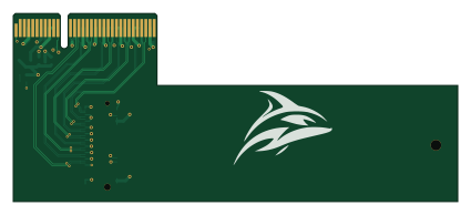
About the ORCA-PCIe-NVMe-Link- PCB
ORCA-PCIe-NVMe-Link- is an open source PCB design by Finn254254, published on GitHub. It is a 6-layer board measuring 106.2 × 44.9 mm, with 8 components from 8 distinct parts.
By type, the board carries 3 capacitors, 2 connectors, 1 fuse, 1 diode and 1 resistor.
From the project
ORCA PCIe NVMe Link is a custom PCIe expansion board that adds M.2 NVMe storage through a PCIe x4 interface. Designed as part of the ORCA hardware platform for high-speed, modular storage expansion.
ORCA PCIe NVMe Link is a custom PCIe expansion board designed by Finn and branded ORCA Servers. It is intended to add M.2 NVMe storage through a PCIe x4 interface as part of the modular ORCA hardware platform.
The design work is complete enough to prepare for prototyping, but physical manufacturing, assembly, independent engineering review and hardware testing still need funding.
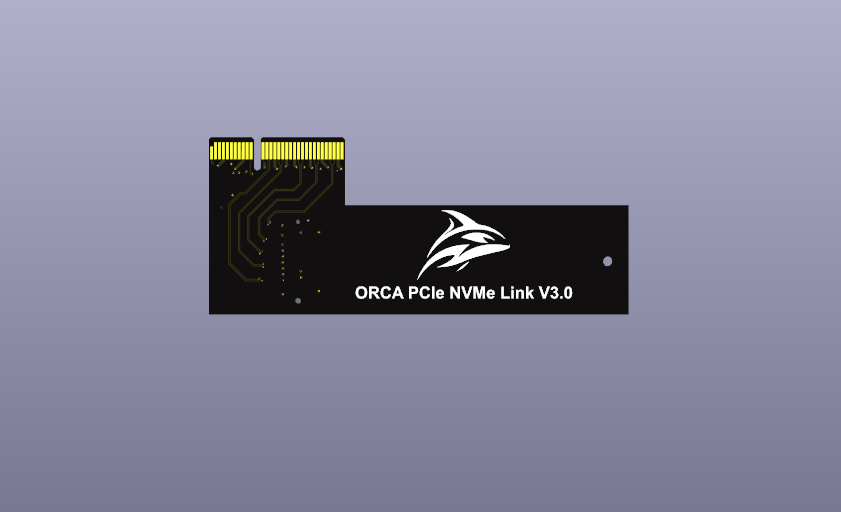
ORCA-PCIe-NVMe-Link- bill of materials (BOM)
8 components, 8 distinct parts — part numbers from the project's BOM.
| Qty | Part | Footprint | Refs |
|---|---|---|---|
| 1 | BUS_PCI_EXPRESS_X4 Bus_PCI_Express_x4 | BUS_PCIexpress_x4 | J1 |
| 1 | BUS_M.2_SOCKET_M Bus_M.2_Socket_M | TE_1-2199119-5 | J2 |
| 1 | 3A | Fuse_1206_3216Metric | F1 |
| 1 | LED | LED_0603_1608Metric | D1 |
| 1 | 10UF 10uF | C_0805_2012Metric | C1 |
| 1 | 100NF 100nF | C_0402_1005Metric | C2 |
| 1 | 22UF 22uF | C_0805_2012Metric | C3 |
| 1 | 1K | R_0603_1608Metric | R1 |
ORCA-PCIe-NVMe-Link- design files
The KiCad project lives in the Finn254254/ORCA-PCIe-NVMe-Link- repository on GitHub; these links point at the commit this page was built from.
ORCA-PCIe-NVMe-Link-: common questions
How big is the ORCA-PCIe-NVMe-Link- PCB?
The ORCA-PCIe-NVMe-Link- measures 106.2 × 44.9 mm, has 6 copper layers and is 1.5584 mm thick.
How many components are on the ORCA-PCIe-NVMe-Link-?
8 components, from 8 distinct parts, with part numbers taken from the project's own BOM. The full bill of materials is listed on this page.
Where can I download the ORCA-PCIe-NVMe-Link- design files?
From the Finn254254/ORCA-PCIe-NVMe-Link- repository on GitHub, which has the KiCad layout, the schematic and the BOM; the links under Design files point to each one.
Can I use the ORCA-PCIe-NVMe-Link- design in my own project?
The repository has no license, so all rights stay with Finn254254. Use it as a reference, and ask the author before reusing the design.