
Pcb

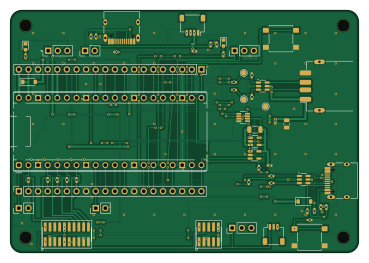
About the Pcb
Pcb is an open source PCB design by hathach, published on GitHub. It is a 2-layer board measuring 92 × 64 mm, with 30 components from 19 distinct parts.
By type, the board carries 9 connectors, 4 jumpers and 1 switch.
From the project
PCB assembly
One repo, Adafruit-style: every board lives in its own directory here, alongside the shared knowledge, footprints, and tooling that future boards reuse. Board pico2tracemotherboard's original 50-commit build history is preserved on branch archive/pico2-original.
Read docs/pipeline.md — short version: copy pico2tracemotherboard/hw/ wholesale, gut the board-specific tables, keep every helper and gate, seed footprints from lib/pcb.pretty/, and regenerate-never-hand-nudge.
Pcb bill of materials (BOM)
30 components, 19 distinct parts — part numbers from the project's BOM.
| Qty | Part | Footprint | Refs |
|---|---|---|---|
| 2 | BREAKOUT | PinSocket_1x20_P2.54mm_Vertical | J1B, J2B |
| 1 | MIPI-20 | FTSH-110-01-DV | J3 |
| 1 | C6307429 USB-A HOST | USB_A_Receptacle_GCT_USB1046 | J5 |
| 1 | CORTEX-10 | FTSH-105-01-DV | J6 |
| 1 | C160403 JST-SH-3 DEBUG_PROBE | JST_SH_SM03B-SRSS-TB_1x03-1MP_P1.00mm_Horizontal | J7 |
| 1 | C165948 USB-C PWR | USB_C_PWR_HRO_TYPE-C-31-M-12 | J8 |
| 1 | C165948 USB-C DEV | USB_C_DEV_HRO_TYPE-C-31-M-12 | J9 |
| 1 | C124376 SWD | PinHeader_1x03_P2.54mm_Vertical | J10 |
| 3 | 100n/16V | C_0402_1005Metric | C_HVBUS_100n, C_P3V3_1, C_P3V3_2 |
| 1 | 1N4148W | D_SOD-123 | D_J9_BUSPWR |
| 1 | C124376 5V SEL | PinHeader_1x03_P2.54mm_Vertical | JP1 |
| 1 | C124375 GP0 GUARD | PinHeader_1x02_P2.54mm_Vertical | JP2 |
| 1 | C124375 GP6 GUARD | PinHeader_1x02_P2.54mm_Vertical | JP3 |
| 1 | C124375 VBUS_DET EN | PinHeader_1x02_P2.54mm_Vertical | JP4 |
| 4 | 5.1k | R_0402_1005Metric | R_CC1, R_CC2, R_CC3, R_CC4 |
| 2 | 8.2k | R_0402_1005Metric | R_J9VD_B, R_J9VD_T |
| 5 | 27 | R_0402_1005Metric | Rt1, Rt2, Rt3, Rt4, Rt5 |
| 1 | C2733655 RESET | SW_SPST_B3S-1000 | SW1 |
| 1 | INA219 | SOT-23-8 | U_INA219_ALT |
Pcb design files
The KiCad project lives in the hathach/pcb repository on GitHub; these links point at the commit this page was built from.
Pcb: common questions
How big is the Pcb?
The Pcb measures 92 × 64 mm, has 2 copper layers and is 1.6 mm thick.
How many components are on the Pcb?
30 components, from 19 distinct parts, with part numbers taken from the project's own BOM. The full bill of materials is listed on this page.
Where can I download the Pcb design files?
From the hathach/pcb repository on GitHub, which has the KiCad layout, the schematic and the BOM; the links under Design files point to each one.
Can I use the Pcb design in my own project?
The repository has no license, so all rights stay with hathach. Use it as a reference, and ask the author before reusing the design.