Patchloop

About the Patchloop PCB
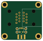
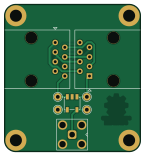
Patchloop is an open source PCB design by hennichodernich, published on GitHub under the Custom license license. It is a 2-layer board measuring 36 × 39 mm, with 8 components from 4 distinct parts.
By type, the board carries 4 test points and 3 connectors.
From the project
Design files for the PatchLoop PCB(s)
The files patchloop2.kicad_* contain the version with RJ45 jacks on opposite sides. This allows for neat short traces between the jacks.
I needed to rework the files patchloop.kicad_* (jacks on same side) because the first version contained a bug so that only one loop was used effectively.
PCB manufacturer Aisler will directly accept the KiCad file for manufacturing, but you can find zipfiles with the gerbers for both variants in the gerbers/ subdirectory. Any PCB manufacturer (e.g. BetaLayout, JLCPCB, PCBWay, OSHPark) should be able to accept those.
Patchloop bill of materials (BOM)
8 components, 4 distinct parts.
| Qty | Part | Footprint | Refs |
|---|---|---|---|
| 2 | 8P8C | RJ45_Amphenol_54602-x08_Horizontal | J1, J3 |
| 1 | Conn_Coaxial | SMA_Amphenol_901-143_Horizontal | J2 |
| 4 | TestPoint | TestPoint_THTPad_D2.0mm_Drill1.0mm | TP1, TP2, TP3, TP4 |
| 1 | ETC4-1-2 | Transformer_MACOM_SM-22 | TR1 |
Patchloop design files
The KiCad project lives in the hennichodernich/patchloop repository on GitHub; these links point at the commit this page was built from.
- Layoutpatchloop.kicad_pcb
- Schematicpatchloop.kicad_sch
Patchloop: common questions
How big is the Patchloop PCB?
The Patchloop measures 36 × 39 mm, has 2 copper layers and is 1.6002 mm thick.
How many components are on the Patchloop?
8 components, from 4 distinct parts. The full bill of materials is listed on this page.
Where can I download the Patchloop design files?
From the hennichodernich/patchloop repository on GitHub, which has the KiCad layout and the schematic; the links under Design files point to each one.
Can I use the Patchloop design in my own project?
It is published under Custom license, which limits how it may be reused; read the license before building on it.