
Out

About the Out PCB
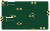
Out is an open source PCB design by ignamv, published on GitHub under the GPL-2.0 license. It is a 2-layer board measuring 40.6 × 24.1 mm, with 10 components from 6 distinct parts.
By type, the board carries 4 resistors, 3 connectors, 2 capacitors and 1 transistor.
From the project
Utility Kicad scripts
Making RFID readers and tags requires designing antenna inductors. This tool simplifies the process by allowing you to quickly analyze PCB spiral inductors with FastHenry to find inductance and Q. Once you're satisfied with a design, you can save a Kicad footprint to incorporate into your PCB layout.
You can use it online at http://ignamv2.linkpc.net/spiral/
For local use, download the folder rfid_calculator and run cmdline.py. Example:

Out bill of materials (BOM)
10 components, 6 distinct parts.
| Qty | Part | Footprint | Refs |
|---|---|---|---|
| 1 | BC547 | TO-92_Inline_Narrow_Oval | Q1 |
| 3 | CONN_01X02 | Pin_Header_Angled_1x02 | P1, P2, P3 |
| 2 | .1u | C_0805_HandSoldering | C1, C2 |
| 2 | 10k | R_0805_HandSoldering | R1, R2 |
| 1 | 200 | R_0805_HandSoldering | R3 |
| 1 | 1k | R_0805_HandSoldering | R4 |
Out design files
The KiCad project lives in the ignamv/kicad_scripts repository on GitHub; these links point at the commit this page was built from.
Out: common questions
How big is the Out PCB?
The Out measures 40.6 × 24.1 mm, has 2 copper layers and is 1.6 mm thick.
How many components are on the Out?
10 components, from 6 distinct parts. The full bill of materials is listed on this page.
Where can I download the Out design files?
From the ignamv/kicad_scripts repository on GitHub, which has the KiCad layout; the links under Design files point to each one.
Can I use the Out design in my own project?
Yes, under the terms of its GPL-2.0 license, which ignamv chose for the repository.
