
Apb

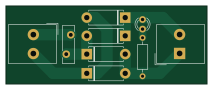
About the Apb PCB
Apb is an open source PCB design by PappasFlow, published on GitHub. It is a 2-layer board measuring 53.1 × 20.6 mm, with 9 components from 5 distinct parts.
By type, the board carries 5 diodes, 2 connectors, 1 fuse and 1 resistor.
Apb bill of materials (BOM)
9 components, 5 distinct parts.
| Qty | Part | Footprint | Refs |
|---|---|---|---|
| 2 | Conn_01x02_Pin | Altech_AK300_1x02_P5.00mm_45-Degree | J1, J2 |
| 1 | Fuse | Fuse_Bourns_MF-RG400 | F1 |
| 4 | D | D_5W_P10.16mm_Horizontal | D1, D2, D3, D4 |
| 1 | LED | LED_D3.0mm | D5 |
| 1 | R | R_Axial_DIN0207_L6.3mm_D2.5mm_P10.16mm_Horizontal | R1 |
Apb design files
The KiCad project lives in the PappasFlow/kicad repository on GitHub; these links point at the commit this page was built from.
- Layoutapb/apb.kicad_pcb
- Schematicapb/apb.kicad_sch
Apb: common questions
How big is the Apb PCB?
The Apb measures 53.1 × 20.6 mm, has 2 copper layers and is 1.6 mm thick.
How many components are on the Apb?
9 components, from 5 distinct parts. The full bill of materials is listed on this page.
Where can I download the Apb design files?
From the PappasFlow/kicad repository on GitHub, which has the KiCad layout and the schematic; the links under Design files point to each one.
Can I use the Apb design in my own project?
The repository has no license, so all rights stay with PappasFlow. Use it as a reference, and ask the author before reusing the design.
More boards in kicad
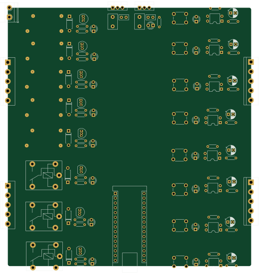 AVR/Arduino
Plc
129 × 137.2 mm110 parts2LNo license0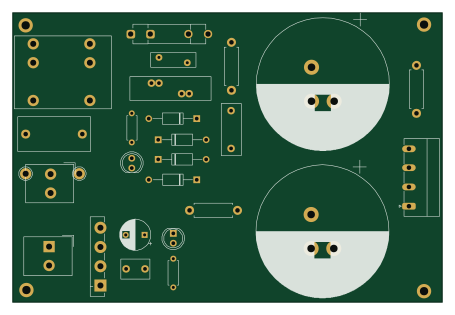
Fuente conmutada
113.7 × 76.6 mm76 parts2LNo license0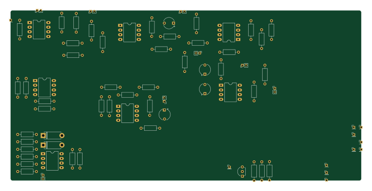
Op
191.1 × 92.6 mm75 parts2LNo license0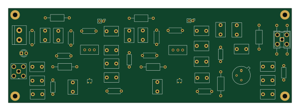
Ampli RF
150 × 50 mm55 parts2LNo license0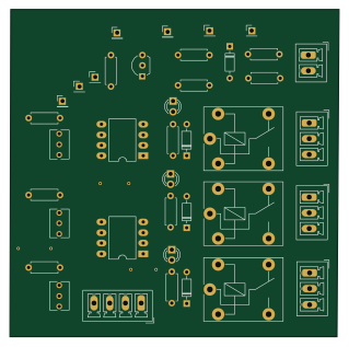
Comparador
79.5 × 79 mm39 parts2LNo license0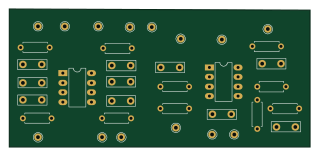
Filtros TCII
79.8 × 36.6 mm36 parts2LNo license0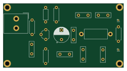
Oscilador Clapp
62.7 × 33.5 mm18 parts2LNo license0
Pwm ka3525
37.1 × 45.5 mm18 parts2LNo license0
Oscilador Hartley
57.1 × 30 mm16 parts2LNo license0
Driver transistor
85.9 × 37.1 mm14 parts2LNo license0