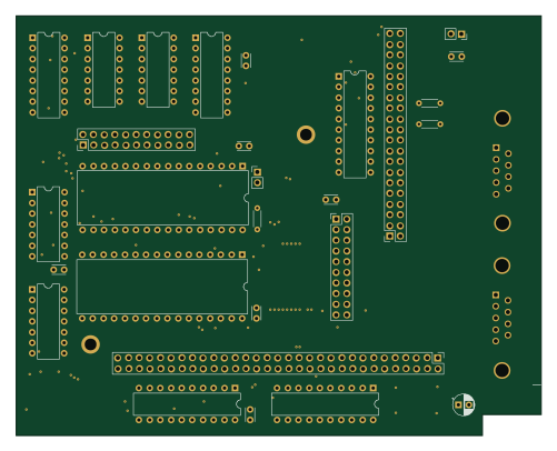
Multi-IO-Daughtercard

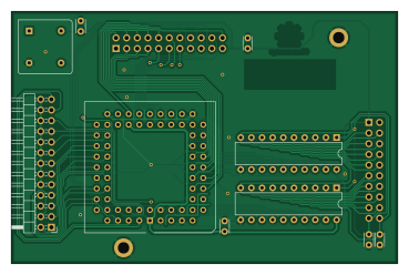
About the Multi-IO-Daughtercard PCB
Multi-IO-Daughtercard is an open source PCB design by rkrenicki, published on GitHub. It is a 2-layer board measuring 92 × 60 mm, with 12 components from 7 distinct parts.
From the project
Variant of the 3-in-1 Expansion board with Dual Serial and a second Parallel port.
This is a single expansion board designed for the Tandy 1000 EX and HX computers, to include the following upgrades:
640KB Base System Memory and 96KB Upper Memory 2x 16550-based DE9 Serial RS232 Ports and 1x Parallel Port * XT-IDE based CompactFlash "Hard Drive"
This board is for the Tandy 1000EX and 1000HX computers only. It will not work in any other computer model as it is. You must remove any expansion cards already in the computer, this is designed to be a single-board upgrade and has no provisions to allow for any other expansion cards.
Multi-IO-Daughtercard bill of materials (BOM)
12 components, 7 distinct parts.
| Qty | Part | Footprint | Refs |
|---|---|---|---|
| 1 | Multi-IO Mezzanine Data/IO | PinSocket_2x11_P2.54mm_Vertical | IO-J1 |
| 1 | Multi-IO Mezzanine Output | PinSocket_2x10_P2.54mm_Vertical | IO-J2 |
| 1 | LPT2 | PinHeader_2x13_P2.54mm_Horizontal | IO-J3 |
| 1 | 1.8432MHz | Oscillator_DIP-8 | IO-OSC1 |
| 1 | 16C552 | PLCC-68_THT-Socket | IO-U1 |
| 2 | GD75232 | DIP-20_W7.62mm | IO-U3, IO-U4 |
| 5 | 0.1uF | C_Disc_D3.0mm_W2.0mm_P2.50mm | C1, C2, C3, C4, C5 |
Multi-IO-Daughtercard design files
The KiCad project lives in the rkrenicki/Tandy-EX-HX-3in1-V2 repository on GitHub; these links point at the commit this page was built from.
Multi-IO-Daughtercard: common questions
How big is the Multi-IO-Daughtercard PCB?
The Multi-IO-Daughtercard measures 92 × 60 mm, has 2 copper layers and is 1.6 mm thick.
How many components are on the Multi-IO-Daughtercard?
12 components, from 7 distinct parts. The full bill of materials is listed on this page.
Where can I download the Multi-IO-Daughtercard design files?
From the rkrenicki/Tandy-EX-HX-3in1-V2 repository on GitHub, which has the KiCad layout and the schematic; the links under Design files point to each one.
Can I use the Multi-IO-Daughtercard design in my own project?
The repository has no license, so all rights stay with rkrenicki. Use it as a reference, and ask the author before reusing the design.