
SP1ETH

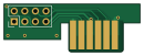
About the SP1ETH PCB
SP1ETH is an open source PCB design by silverstee1, published on GitHub under the Unlicense license. It is a 2-layer board measuring 32.5 × 11.5 mm, with 2 components from 2 distinct parts.
From the project
DIY Adapter PCB and Case for SP1 on the Gamecube for a ENC28J60 BBA
Must be used with the lastest version of Swiss as of 1788 in order to use the in game BBA features as it supports the hypervisor driver for games.
Must be ordered from fab such as jlcpcb with 1.2mm thickness with ENIG surface finish
I used 10CM Female to Male dupont wires to connect the ENC28J60 Mini to the pcb but regular wires can be directly soldered to the pcb and ENC28J60 as well, make sure to follow the pinout below.
SP1ETH bill of materials (BOM)
2 components, 2 distinct parts.
| Qty | Part | Footprint | Refs |
|---|---|---|---|
| 1 | Serial Port 1 | SP1_FootPrint | J1 |
| 1 | Conn_02x04_Odd_Even | PinHeader_2x04_P2.54mm_Vertical | J2 |
SP1ETH design files
The KiCad project lives in the silverstee1/SP1ETH repository on GitHub; these links point at the commit this page was built from.
- LayoutKicad/ConnSP1.kicad_pcb
- SchematicKicad/ConnSP1.kicad_sch
SP1ETH: common questions
How big is the SP1ETH PCB?
The SP1ETH measures 32.5 × 11.5 mm, has 2 copper layers and is 1.6 mm thick.
How many components are on the SP1ETH?
2 components, from 2 distinct parts. The full bill of materials is listed on this page.
Where can I download the SP1ETH design files?
From the silverstee1/SP1ETH repository on GitHub, which has the KiCad layout and the schematic; the links under Design files point to each one.
Can I use the SP1ETH design in my own project?
Yes, under the terms of its Unlicense license, which silverstee1 chose for the repository.