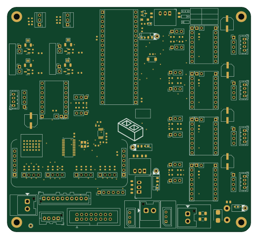
Distribution Layer Adapter Board PCBA

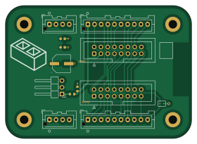
About the Distribution Layer Adapter Board PCBA
Distribution Layer Adapter Board PCBA is an open source PCB design by basicallysource, published on GitHub. It is a 2-layer board measuring 70 × 50 mm, with 12 components from 11 distinct parts.
By type, the board carries 7 connectors, 3 capacitors and 2 resistors.
From the project
Edit the YAML, push, open a PR. That's the whole workflow: no toolchain, no credentials, no publish step to remember. The PR's docs preview shows the PR's own drawings about 90 seconds after each push.
Edit the YAML, push, open a PR. That's the whole workflow: no toolchain, no credentials, no publish step to remember. The PR's docs preview shows the PR's own drawings about 90 seconds after each push.
To look at a drawing before pushing, render it yourself:
Everything lands in wireharness/out/`, which is gitignored: a local render can never end up committed, even by accident. CI's render is still the canonical one (its graphviz is pinned; yours probably differs by a pixel or two, and the next CI run quietly normalizes the published copy).
Distribution Layer Adapter Board PCBA bill of materials (BOM)
12 components, 11 distinct parts — part numbers from the project's BOM.
| Qty | Part | Footprint | Refs |
|---|---|---|---|
| 2 | C2937625 Conn_01x10 XFCN | JST_XA_B10B-XASK-1-A_1x10_P2.50mm_Vertical | J1, J2 |
| 1 | C131334 Conn_02x08_Odd_Even JST | IDC-Header_2x08_P2.54mm_Vertical | J3 |
| 1 | C2691448 Conn_02x08_Odd_Even XFCN | IDC-Header_2x08_P2.54mm_Vertical | J4 |
| 1 | C27438 Conn_01x03 BOOMELE(Boom Precision Elec) | PinHeader_1x03_P2.54mm_Horizontal | J5 |
| 1 | C49661 Conn_01x04 BOOMELE(Boom Precision Elec) | JST_XA_B04B-XASK-1-A_1x04_P2.50mm_Vertical | J6 |
| 1 | C27438 Conn_01x04 BOOMELE(Boom Precision Elec) | JST_XA_B04B-XASK-1-A_1x04_P2.50mm_Vertical | J7 |
| 1 | C242100 100uF Panasonic | CAP-SMD_BD6.3-L6.6-W6.6-LS7.4-FD | C1 |
| 1 | C242100 1uF Samsung Electro-Mechanics | C_0603 | C2 |
| 1 | C242100 100nF YAGEO | C_0603 | C3 |
| 1 | C84376 0Ω UNI-ROYAL(Uniroyal Elec) | R_0603 | R1 |
| 1 | C95781 10kΩ UNI-ROYAL(Uniroyal Elec) | R_0603 | R3 |
Distribution Layer Adapter Board PCBA design files
The KiCad project lives in the basicallysource/sorter-v2 repository on GitHub; these links point at the commit this page was built from.
Distribution Layer Adapter Board PCBA: common questions
How big is the Distribution Layer Adapter Board PCBA?
The Distribution Layer Adapter Board PCBA measures 70 × 50 mm, has 2 copper layers and is 1.6 mm thick.
How many components are on the Distribution Layer Adapter Board PCBA?
12 components, from 11 distinct parts, with part numbers taken from the project's own BOM. The full bill of materials is listed on this page.
Where can I download the Distribution Layer Adapter Board PCBA design files?
From the basicallysource/sorter-v2 repository on GitHub, which has the KiCad layout, the schematic and the BOM; the links under Design files point to each one.
Can I use the Distribution Layer Adapter Board PCBA design in my own project?
The repository has no license, so all rights stay with basicallysource. Use it as a reference, and ask the author before reusing the design.