
Novalink

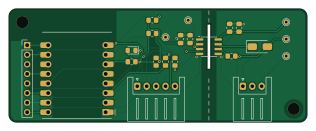
About the Novalink PCB
Novalink is an open source PCB design by benbox69, published on GitHub under the CC-BY-NC-4.0 license. It is a 2-layer board measuring 79 × 30 mm, with 17 components from 11 distinct parts.
Other key parts include the CA-IS3721HS. By type, the board carries 7 resistors, 4 capacitors, 3 connectors, 1 IC, 1 LED and 1 diode.
From the project
NovaLink: isolated ESP32-C3 interface for Micronova pellet stoves (NAVEL INSIDE port) - KiCad 10, JLCPCB-ready, 3D-printable enclosure
Galvanically isolated ESP32-C3 interface for Micronova-controlled pellet stoves (NAVEL INSIDE port).
NovaLink plugs into the 3-pin service port of a Micronova stove board (designed for X100 EVO "NAVEL INSIDE" connector, +5 V / SER / GND, 19200 baud single-wire serial) and lets an ESP32-C3 SuperMini talk to the stove through a 3.75 kV digital isolator. The stove side is powered by the stove itself; the ESP side is powered by USB-C. An optional VL53L0X time-of-flight sensor can be connected (for example to measure the pellet level).
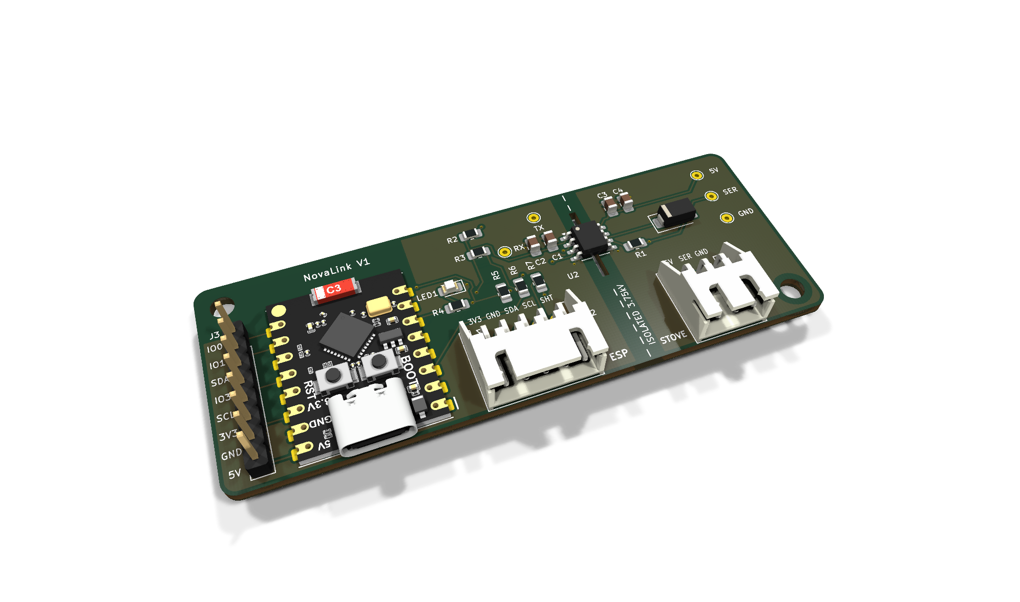
Main components on the Novalink
Novalink bill of materials (BOM)
17 components, 11 distinct parts — part numbers from the project's BOM.
| Qty | Part | Footprint | Refs |
|---|---|---|---|
| 1 | CA-IS3721HS Chipanalog | SOIC-8_3.9x4.9mm_P1.27mm | U2 |
| 1 | S3B-XH-A(LF)(SN) NAVEL_INSIDE JST | JST_XH_S3B-XH-A_1x03_P2.50mm_Horizontal | J1 |
| 1 | S5B-XH-A(LF)(SN) TOF_SENSOR JST | JST_XH_S5B-XH-A_1x05_P2.50mm_Horizontal | J2 |
| 1 | PZ254V-11-08P EXTENSION XFCN | PinHeader_1x08_P2.54mm_Vertical | J3 |
| 1 | NCD0805R1 RED Nationstar | LED_0805_2012Metric_Pad1.15x1.40mm_HandSolder | LED1 |
| 1 | SS14 MDD | D_SMA | D1 |
| 2 | 100NF 100nF | C_0805_2012Metric_Pad1.18x1.45mm_HandSolder | C1, C3 |
| 2 | C28323 1µF | C_0805_2012Metric_Pad1.18x1.45mm_HandSolder | C2, C4 |
| 2 | 0805W8F1001T5E 1k UNI-ROYAL | R_0805_2012Metric_Pad1.20x1.40mm_HandSolder | R1, R4 |
| 2 | 2.2K 2.2k | R_0805_2012Metric_Pad1.20x1.40mm_HandSolder | R2, R3 |
| 3 | 0805W8F1000T5E 100 UNI-ROYAL | R_0805_2012Metric_Pad1.20x1.40mm_HandSolder | R5, R6, R7 |
Novalink design files
The KiCad project lives in the benbox69/novalink repository on GitHub; these links point at the commit this page was built from.
- LayoutNovaLink.kicad_pcb
- SchematicNovaLink.kicad_sch
- BOMproduction/bom.csv
Novalink: common questions
How big is the Novalink PCB?
The Novalink measures 79 × 30 mm, has 2 copper layers and is 1.6 mm thick.
How many components are on the Novalink?
17 components, from 11 distinct parts, with part numbers taken from the project's own BOM. The full bill of materials is listed on this page.
Where can I download the Novalink design files?
From the benbox69/novalink repository on GitHub, which has the KiCad layout, the schematic and the BOM; the links under Design files point to each one.
Can I use the Novalink design in my own project?
It is published under CC-BY-NC-4.0, which limits how it may be reused; read the license before building on it.