
Task1

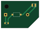
About the Task1 PCB
Task1 is an open source PCB design by dae9999nam, published on GitHub. It is a 2-layer board measuring 35 × 25 mm, with 4 components from 4 distinct parts.
By type, the board carries 1 battery holder, 1 switch, 1 diode and 1 resistor.
It belongs with the iot & wireless designs in this gallery.
From the project
This repository is to record comprehensive learning of technology and package from ELEC2840
Task1 bill of materials (BOM)
4 components, 4 distinct parts.
| Qty | Part | Footprint | Refs |
|---|---|---|---|
| 1 | 103(CR2032) | BatteryHolder_Keystone_103_1x20mm | BT1 |
| 1 | SW_Push | SW_SPST_CK_RS282G05A3 | SW1 |
| 1 | Red | LED_1210_3225Metric | D1 |
| 1 | 300R | R_1206_3216Metric | R1 |
Task1 design files
The KiCad project lives in the dae9999nam/SL_Blog repository on GitHub; these links point at the commit this page was built from.
- LayoutPCB/Day1/task1.kicad_pcb
Task1: common questions
How big is the Task1 PCB?
The Task1 measures 35 × 25 mm, has 2 copper layers and is 1.6 mm thick.
How many components are on the Task1?
4 components, from 4 distinct parts. The full bill of materials is listed on this page.
Where can I download the Task1 design files?
From the dae9999nam/SL_Blog repository on GitHub, which has the KiCad layout; the links under Design files point to each one.
Can I use the Task1 design in my own project?
The repository has no license, so all rights stay with dae9999nam. Use it as a reference, and ask the author before reusing the design.
More boards in SL_Blog
Similar boards
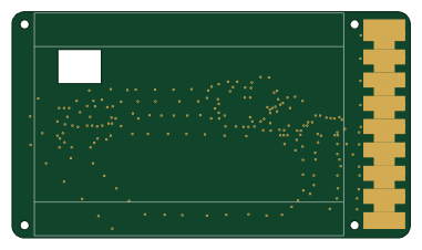
EinkPDA screen
TalismanDesign
95 × 54 mm27 parts2LApache-2.02.0k
RPi RM0 WiFi/Bluetooth Module
schlae
11.1 × 14 mm76 parts6LNo license1.0k
L0 USB
Luos-io
20.3 × 15.3 mm19 parts2LMIT547
Breakout board
26.7 × 27.9 mm29 parts2LMIT547
Stm32f0 disco Luos shield
55.9 × 99.1 mm26 parts2LMIT547
L0 USBA
20.3 × 15.3 mm19 parts2LMIT547