Tweezer tips


About the Tweezer tips PCB
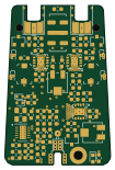
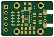
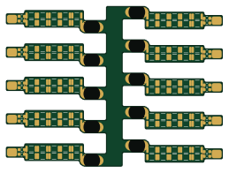
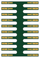
Tweezer tips is an open source PCB design by devEmbedded, published on GitHub. It is a 2-layer board measuring 121.1 × 8 mm, with 9 components from 8 distinct parts.
By type, the board carries 3 connectors, 2 capacitors and 2 resistors.
From the project
Modular differential probe (DEDP-100)
Modular differential probe (DEDP-100) =====================================
This repository contains the design files of a 100 MHz differential probe for use with oscilloscopes. The design is modular and consists of a base amplifier unit with exchangeable probe tip accessories. The accessory can be chosen to fit the desired voltage range and connection type.
Currently this project is still in development. While the prototype revisions work well, they are still being redesigned for improvements.
Tweezer tips bill of materials (BOM)
9 components, 8 distinct parts.
| Qty | Part | Footprint | Refs |
|---|---|---|---|
| 1 | TIP | SIMPLE_PAD | J1 |
| 1 | TO_AMP | SIMPLE_PAD | J2 |
| 1 | GND | SIMPLE_PAD | J3 |
| 2 | SPARK_GAP | PCB_SPARK_GAP | E1, E2 |
| 1 | 1.0pF | C_0603_1608Metric | C1 |
| 1 | N/A | C_0603_1608Metric | C2 |
| 1 | 9.53M | R_0603_1608Metric | R1 |
| 1 | 220 | R_0603_1608Metric | R2 |
Tweezer tips design files
The KiCad project lives in the devEmbedded/differential_probe repository on GitHub; these links point at the commit this page was built from.
Tweezer tips: common questions
How big is the Tweezer tips PCB?
The Tweezer tips measures 121.1 × 8 mm, has 2 copper layers and is 1 mm thick.
How many components are on the Tweezer tips?
9 components, from 8 distinct parts. The full bill of materials is listed on this page.
Where can I download the Tweezer tips design files?
From the devEmbedded/differential_probe repository on GitHub, which has the KiCad layout; the links under Design files point to each one.
Can I use the Tweezer tips design in my own project?
The repository has no license, so all rights stay with devEmbedded. Use it as a reference, and ask the author before reusing the design.