
P11


About the P11 PCB
P11 is an open source PCB design by DushyantSingh27, published on GitHub. It is a 2-layer board measuring 6.8 × 8.1 mm, with 8 components from 1 distinct parts.
From the project
LLM Driven End to End PCB Generation for KiCAD
Turn a natural-language circuit description into an ERC-clean KiCad 9 schematic and a DRC-checked, routed PCB — headless, no GUI step anywhere in the flow.
Design intent is guided by STMicroelectronics hardware design guidelines, with mentorship from ST engineers on layout practice. Manufacturability limits come from a fabricator's DFM specification. KiCad is treated as the single source of truth for every file format, and KiCad's own ERC and DRC verify the output independently of the code that produced it.
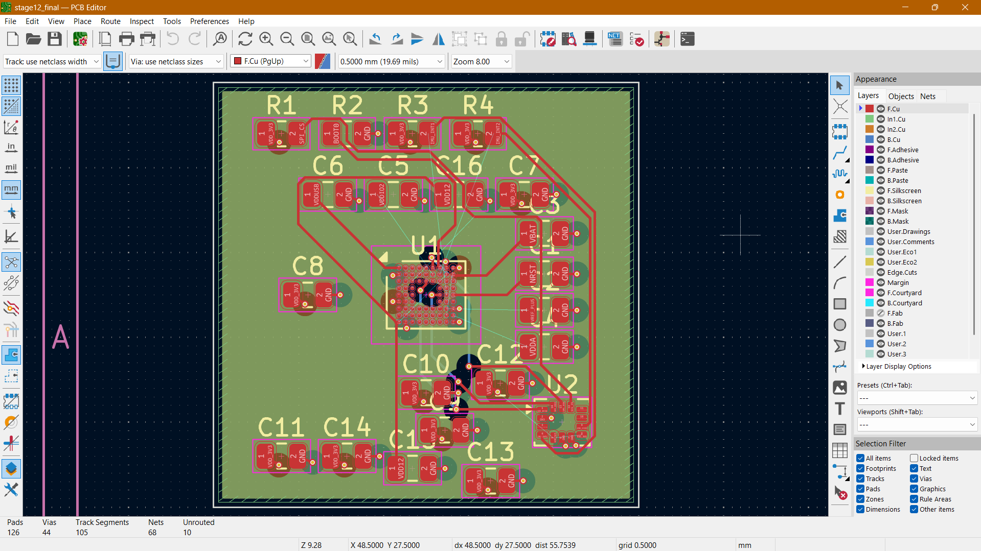
P11 bill of materials (BOM)
8 components, 1 distinct parts.
| Qty | Part | Footprint | Refs |
|---|---|---|---|
| 8 | 100nF | C_0805 | C1, C2, C3, C4, C5, C6, C7, C8 |
P11 design files
The KiCad project lives in the DushyantSingh27/LLM-Driven-End-to-End-PCB-Generation-for-KiCAD repository on GitHub; these links point at the commit this page was built from.
P11: common questions
How big is the P11 PCB?
The P11 measures 6.8 × 8.1 mm, has 2 copper layers and is 1.6 mm thick.
How many components are on the P11?
8 components, from 1 distinct parts. The full bill of materials is listed on this page.
Where can I download the P11 design files?
From the DushyantSingh27/LLM-Driven-End-to-End-PCB-Generation-for-KiCAD repository on GitHub, which has the KiCad layout; the links under Design files point to each one.
Can I use the P11 design in my own project?
The repository has no license, so all rights stay with DushyantSingh27. Use it as a reference, and ask the author before reusing the design.
More boards in LLM-Driven-End-to-End-PCB-Generation-for-KiCAD
P17
25.1 × 26.1 mm34 parts2LNo license0
Extracted task 17
41 × 43.2 mm27 parts2LNo license0
P16
18 × 19.9 mm22 parts2LNo license0
P6
11.1 × 12.4 mm11 parts2LNo license0
P15
11.1 × 11.7 mm10 parts2LNo license0
P12
6.8 × 8.1 mm8 parts2LNo license0
P9
6.8 × 8.1 mm8 parts2LNo license0
P8
6.8 × 8.1 mm8 parts2LNo license0
P14
11.1 × 11.7 mm8 parts2LNo license0
P10
6.8 × 8.1 mm8 parts2LNo license0
P3
6.2 × 8.9 mm6 parts2LNo license0