
Dev

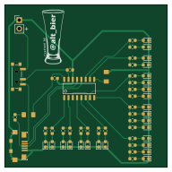
About the Dev PCB
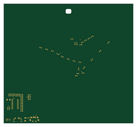
Dev is an open source PCB design by gowenrw, published on GitHub under the MIT license. It is a 2-layer board measuring 48 × 48 mm, with 57 components from 12 distinct parts.
Other key parts include the IC_CH552G. By type, the board carries 25 resistors, 24 diodes, 3 switches, 2 connectors, 2 capacitors and 1 IC.
It belongs with the wearables designs in this gallery.
From the project
84 Badge
KiCad project folder for initial development PCB(s)
This is the file structure of this repository
/ - Home /eda - Electronic Design Automation files (i.e. KiCad) /eda/dev/ - YOU ARE HERE ./.pro - project file. Holds parameters that apply to the entire project (e.g. schematic, PCB layout, etc.). ./.sch - schematic file. ./.kicadpcb - the PCB New layout file. ./.net - netlist in "Pcbnew" format ./.bak - backup of schematic file. ./.kicadpcb-bak - backup of the new PCB layout file. ./-cache.lib - a local cache copy of all the symbols used in the schematic ./fp-lib-table - Footprint library…
Main components on the Dev
Dev bill of materials (BOM)
57 components, 12 distinct parts.
| Qty | Part | Footprint | Refs |
|---|---|---|---|
| 1 | IC_CH552G | IC_SOIC-16_3.9x9.9mm_Pitch1.27mm | IC1 |
| 1 | USB_B_Micro | USB_Micro-B_Jing | J1 |
| 1 | Conn_01x02 | Conn_Pin_Header_Straight_1x02_Pitch2.54mm | J2 |
| 1 | SW_TS2306A | SW_TS2306A240GFMSM9_C388290 | S11 |
| 1 | SPDT_C136659 | SW_SPDT_PCM12_C136659 | SW1 |
| 1 | TS2306A | SW_TS2306A240GFMSM9_C388290 | SW2 |
| 8 | Blue | LED_0603_1608Metric | D141, D142, D161, D162, D171, D172, D321, D322 |
| 8 | Yellow | LED_0603_1608Metric | D151, D152, D153, D154, D301, D302, D303, D304 |
| 8 | Red | LED_0603_1608Metric | D311, D312, D313, D314, D331, D332, D341, D342 |
| 2 | 0.1uF/100nF | C_0603_1608Metric | C1, C2 |
| 1 | 10k Ohms | R_0603_1608Metric | R1 |
| 24 | 220 Ohms | R_0603_1608Metric | R141, R142, R151, R152, R153, R154, R161, R162 +16 |
Dev design files
The KiCad project lives in the gowenrw/84_Badge repository on GitHub; these links point at the commit this page was built from.
- Layouteda/dev/dev.kicad_pcb
Dev: common questions
How big is the Dev PCB?
The Dev measures 48 × 48 mm, has 2 copper layers and is 1.6 mm thick.
How many components are on the Dev?
57 components, from 12 distinct parts. The full bill of materials is listed on this page.
Where can I download the Dev design files?
From the gowenrw/84_Badge repository on GitHub, which has the KiCad layout; the links under Design files point to each one.
Can I use the Dev design in my own project?
Yes, under the terms of its MIT license, which gowenrw chose for the repository.
More boards in 84_Badge
Similar boards
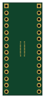
BM28B0.6-24DSBreakout
scottbez1
15.2 × 35.6 mm3 parts2LApache-2.022.2k
LevelShifterBreakout
15.2 × 20.3 mm5 parts2LApache-2.022.2k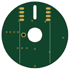
View screen
35 × 35 mm12 parts2LApache-2.022.2k
View base
81.2 × 81.2 mm81 parts2LApache-2.022.2k
ChainlinkBase
98.4 × 190.5 mm119 parts2LApache-2.04.2k
ChainlinkDriverTester
198.1 × 95.3 mm123 parts2LApache-2.04.2k