
Trace width jlc

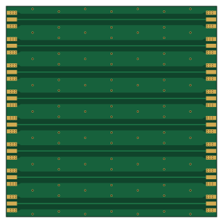
About the Trace width jlc PCB
Trace width jlc is an open source PCB design by greatscottgadgets, published on GitHub under the GPL-2.0 license. It is a 6-layer board measuring 80 × 80 mm, with 12 components from 1 distinct parts.
From the project
miscellaneous Great Scott Gadgets projects
Trace width jlc bill of materials (BOM)
12 components, 1 distinct parts.
| Qty | Part | Footprint | Refs |
|---|---|---|---|
| 12 | CONN_COAXIAL | Linx_SMA_CONSMA003.062 | J1, J2, J3, J4, J5, J6, J7, J8 +4 |
Trace width jlc design files
The KiCad project lives in the greatscottgadgets/misc repository on GitHub; these links point at the commit this page was built from.
Trace width jlc: common questions
How big is the Trace width jlc PCB?
The Trace width jlc measures 80 × 80 mm, has 6 copper layers and is 1.6 mm thick.
How many components are on the Trace width jlc?
12 components, from 1 distinct parts. The full bill of materials is listed on this page.
Where can I download the Trace width jlc design files?
From the greatscottgadgets/misc repository on GitHub, which has the KiCad layout; the links under Design files point to each one.
Can I use the Trace width jlc design in my own project?
Yes, under the terms of its GPL-2.0 license, which greatscottgadgets chose for the repository.
More boards in misc
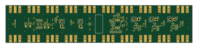
Limiters
100 × 20 mm143 parts4LGPL-2.021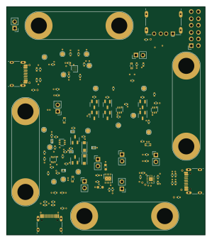
Vbus switch
74 × 85 mm109 parts4LGPL-2.021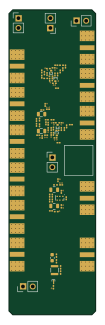
Baluns
23 × 81 mm92 parts4LGPL-2.021
Si5351A
100 × 70 mm80 parts4LGPL-2.021
Rf switch sp4t
164 × 25 mm73 parts4LGPL-2.021
Rf amps
23 × 75 mm59 parts4LGPL-2.021
Passives
100 × 20 mm59 parts4LGPL-2.021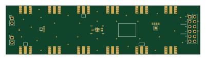
Rf switch sp3t
100 × 25 mm33 parts4LGPL-2.021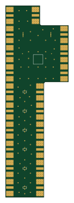
Filters
32.9 × 100 mm32 parts4LGPL-2.021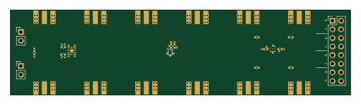
Rf switch dpdt
100 × 25 mm29 parts4LGPL-2.021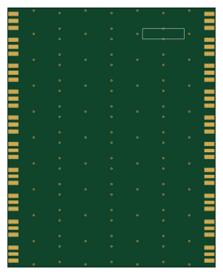
Sma jlc
80 × 100 mm20 parts6LGPL-2.021