
Fpga mcu dac adc conversion pipeline

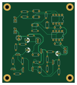
About the Fpga mcu dac adc conversion pipeline PCB
Fpga mcu dac adc conversion pipeline is an open source PCB design by gulotmg, published on GitHub under the MIT license. It is a 2-layer board measuring 62 × 69 mm, with 40 components from 17 distinct parts.
Other key parts include the MCP6021. By type, the board carries 15 resistors, 11 capacitors, 7 transistors, 2 ICs and 1 diode.
From the project
500 kSPS acquisition pipeline: Spartan-7 DDS + DAC7311 + STM32 bare-metal ADC + LabVIEW spectral analysis (IEEE 1241-2023)
Custom 2-layer hardware PCB engineered to replace the baseline passive RC filter with a 4th-order unity-gain Sallen-Key active low-pass filter ($f_0 \approx 79.58\text{ kHz}$, $-80\text{ dB/decade}$ roll-off) powered by an isolated discrete linear series pass regulator.
Designed in KiCad 10.0.6, simulated in LTspice.
While using an off-the-shelf monolithic LDO (such as an LM317, L7805, or LP2985) would have been more straightforward, designing a custom discrete series pass regulator was deliberately chosen for educational satisfaction since calculating thermal drift compensation…
Main components on the Fpga mcu dac adc conversion pipeline
Fpga mcu dac adc conversion pipeline bill of materials (BOM)
40 components, 17 distinct parts.
| Qty | Part | Footprint | Refs |
|---|---|---|---|
| 2 | MCP6021 | DIP-8_W7.62mm | U1, U2 |
| 6 | 2N2222 | TO-92Flat | Q1, Q2, Q3, Q4, Q5, Q6 |
| 1 | 2N3906 | TO-92_Inline | Q7 |
| 1 | 10 | R_Axial_DIN0204_L3.6mm_D1.6mm_P5.08mm_Horizontal | RSENSE1 |
| 3 | Conn_01x02_Pin | PinHeader_1x02_P2.54mm_Vertical | VCC1, VDAC1, VOUT1 |
| 1 | LED | LED_D4.0mm | D1 |
| 5 | 1n | C_Disc_D5.0mm_W2.5mm_P5.00mm | C1, C2, C3, C4, C5 |
| 3 | 47µ | CP_Radial_D4.0mm_P1.50mm | C6, C7, C11 |
| 3 | 100n | C_Disc_D5.0mm_W2.5mm_P5.00mm | C8, C9, C10 |
| 4 | 2k | R_Axial_DIN0204_L3.6mm_D1.6mm_P5.08mm_Horizontal | R1, R2, R3, R4 |
| 4 | 1000 | R_Axial_DIN0204_L3.6mm_D1.6mm_P5.08mm_Horizontal | R5, R10, R13, R15 |
| 1 | 10000 | R_Axial_DIN0204_L3.6mm_D1.6mm_P5.08mm_Horizontal | R6 |
| 1 | 470 | R_Axial_DIN0204_L3.6mm_D1.6mm_P5.08mm_Horizontal | R7 |
| 1 | 5.1k | R_Axial_DIN0204_L3.6mm_D1.6mm_P5.08mm_Horizontal | R8 |
| 2 | 330 | R_Axial_DIN0204_L3.6mm_D1.6mm_P5.08mm_Horizontal | R9, R12 |
| 1 | 2000 | R_Axial_DIN0204_L3.6mm_D1.6mm_P5.08mm_Horizontal | R11 |
| 1 | 220 | R_Axial_DIN0204_L3.6mm_D1.6mm_P5.08mm_Horizontal | R14 |
Fpga mcu dac adc conversion pipeline design files
The KiCad project lives in the gulotmg/fpga-mcu-dac-adc-conversion-pipeline repository on GitHub; these links point at the commit this page was built from.
- Layoutfilter/pcb/filter.kicad_pcb
- Schematicfilter/pcb/filter.kicad_sch
Fpga mcu dac adc conversion pipeline: common questions
How big is the Fpga mcu dac adc conversion pipeline PCB?
The Fpga mcu dac adc conversion pipeline measures 62 × 69 mm, has 2 copper layers and is 1.6 mm thick.
How many components are on the Fpga mcu dac adc conversion pipeline?
40 components, from 17 distinct parts. The full bill of materials is listed on this page.
Where can I download the Fpga mcu dac adc conversion pipeline design files?
From the gulotmg/fpga-mcu-dac-adc-conversion-pipeline repository on GitHub, which has the KiCad layout and the schematic; the links under Design files point to each one.
Can I use the Fpga mcu dac adc conversion pipeline design in my own project?
Yes, under the terms of its MIT license, which gulotmg chose for the repository.