
Test

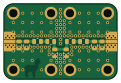
About the Test PCB
Test is an open source PCB design by Halogenek, published on GitHub under the CC-BY-SA-4.0 license. It is a 2-layer board measuring 30 × 20 mm, with 20 components from 3 distinct parts.
From the project
Cheap and simple setup for learning RF electronics
I came across an awesome system for rapid prototyping RF and Microwave solutions by connecting individual components on small PCBs, just like LEGO. This Modular building block system for RF and microwave design of prototypes is in my opinion a very clever way of building RF circuits. On their website the sell almost every available modern RF IC or passive network in a form of a rectangle PCBs.
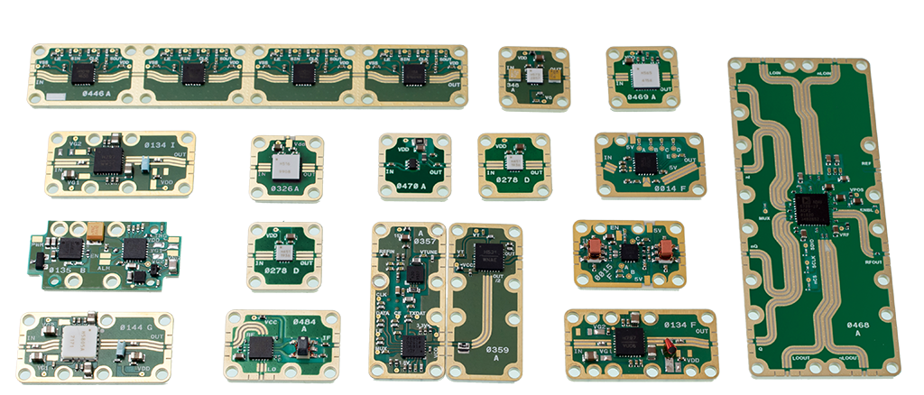
Test bill of materials (BOM)
20 components, 3 distinct parts.
| Qty | Part | Footprint | Refs |
|---|---|---|---|
| 2 | CONN | edge-connector | J1, J2 |
| 8 | M2 | M2-hole | H1, H2, H3, H4, H5, H6, H7, H8 |
| 10 | Z | R_0805_2012Metric | Z1, Z2, Z3, Z4, Z5, Z6, Z7, Z8 +2 |
Test design files
The KiCad project lives in the Halogenek/modular-rf-bench repository on GitHub; these links point at the commit this page was built from.
Test: common questions
How big is the Test PCB?
The Test measures 30 × 20 mm, has 2 copper layers and is 0.8 mm thick.
How many components are on the Test?
20 components, from 3 distinct parts. The full bill of materials is listed on this page.
Where can I download the Test design files?
From the Halogenek/modular-rf-bench repository on GitHub, which has the KiCad layout; the links under Design files point to each one.
Can I use the Test design in my own project?
Yes, under the terms of its CC-BY-SA-4.0 license, which Halogenek chose for the repository.
More boards in modular-rf-bench
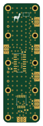
019-Tayloe Quadrature Product Detector
20 × 65 mm29 parts2LCC-BY-SA-4.02
Bjt amp
20 × 20 mm26 parts2LCC-BY-SA-4.02
006-Filter
30 × 20 mm20 parts2LCC-BY-SA-4.02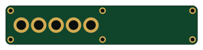
014-base power board
99 × 20 mm16 parts2LCC-BY-SA-4.02
017-Johnson Counter
20 × 20 mm12 parts2LCC-BY-SA-4.02
010 - Amplifier
15 × 20 mm11 parts2LCC-BY-SA-4.02
015-3 Port Resistive Splitter
20 × 20 mm10 parts2LCC-BY-SA-4.02
004-PCB Turn 45
20 × 20 mm6 parts2LCC-BY-SA-4.02
002-SMA Connector
15 × 20 mm6 parts2LCC-BY-SA-4.02
013-prototype board
20 × 40 mm5 parts2LCC-BY-SA-4.02