
Photo single

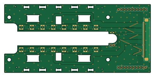
About the Photo single PCB
Photo single is an open source PCB design by hisashin, published on GitHub under the GPL-3.0 license. It is a 2-layer board measuring 123.1 × 58 mm, with 37 components from 5 distinct parts.
By type, the board carries 32 diodes and 1 connector.
From the project
Open source Real-Time Quantitative PCR Implementation

Photo single bill of materials (BOM)
37 components, 5 distinct parts — part numbers from the project's BOM.
| Qty | Part | Footprint | Refs |
|---|---|---|---|
| 1 | Conn_01x60_Male | FFC_60_Ali_HUISHUNFA | J1 |
| 2 | Conn_01x10_Male | Pin_Header_Straight_1x10_Pitch2.54mm | JLN1, JLS1 |
| 1 | Thermistor | R_0603_HandSoldering | TH1 |
| 1 | Thermistor | PinHeader_1x02_P2.54mm_Vertical | TH2 |
| 32 | D_Photo | D_1206_nosilk | D1A1, D1B1, D2A1, D2B1, D3A1, D3B1, D4A1, D4B1 +24 |
Photo single design files
The KiCad project lives in the hisashin/qNinja repository on GitHub; these links point at the commit this page was built from.
Photo single: common questions
How big is the Photo single PCB?
The Photo single measures 123.1 × 58 mm, has 2 copper layers and is 1.6 mm thick.
How many components are on the Photo single?
37 components, from 5 distinct parts, with part numbers taken from the project's own BOM. The full bill of materials is listed on this page.
Where can I download the Photo single design files?
From the hisashin/qNinja repository on GitHub, which has the KiCad layout, the schematic and the BOM; the links under Design files point to each one.
Can I use the Photo single design in my own project?
Yes, under the terms of its GPL-3.0 license, which hisashin chose for the repository.
More boards in qNinja
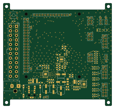
QPCR-main
100 × 94.8 mm92 parts2LGPL-3.047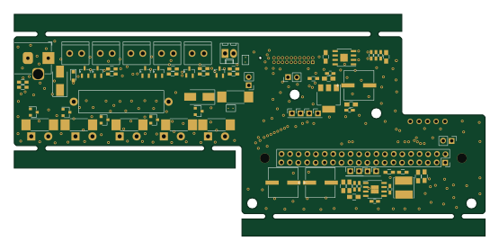 Raspberry Pi
QPCR-root
138.5 × 65.2 mm85 parts2LGPL-3.047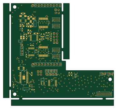
QPCR-photosensing
93.1 × 86.1 mm62 parts2LGPL-3.047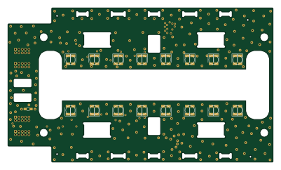
QPCR-photodiode series
100 × 58 mm38 parts2LGPL-3.047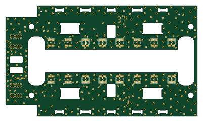
QPCR-photodiode
100 × 58 mm38 parts2LGPL-3.047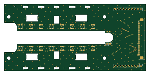
Photo dual
123.1 × 58 mm37 parts2LGPL-3.047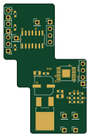 AVR/Arduino
Stepper
31 × 49 mm28 parts2LGPL-3.047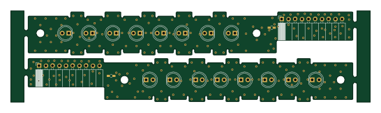
QPCR-panel led 20210831
136.3 × 34.8 mm18 parts2LGPL-3.047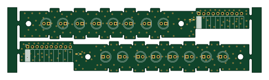
QPCR-panel led 20211208
136.3 × 35.2 mm18 parts2LGPL-3.047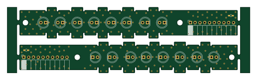
QPCR-panel led 20210629
128.7 × 34.8 mm18 parts2LGPL-3.047