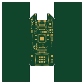
Alpakka

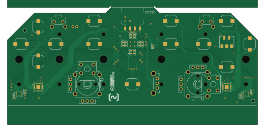
About the Alpakka PCB
Alpakka is an open source PCB design by inputlabs, published on GitHub under the Custom license license. It is a 2-layer board measuring 130 × 61 mm, with 61 components from 33 distinct parts.
Other key parts include the Alpsalpine_RKJXV, Alpsalpine_EC10E, NXP_PCAL6416A and ST_LSM6. By type, the board carries 19 switches, 8 test points, 7 ICs, 5 connectors, 5 resistors and 4 diodes.
From the project
Printed Circuit Board schematics
Alpakka controller Printed Circuit Board reference design
- Open .kicadsch file in Schematics editor. - Go to menu Tools → Edit symbol fields - Group by field Group - Change id references (LCSC id` for JLCPCB).
- After loading the PCB project: Edit → Fill all zones. - Before saving the PCB project: Edit → Unfill all zones.
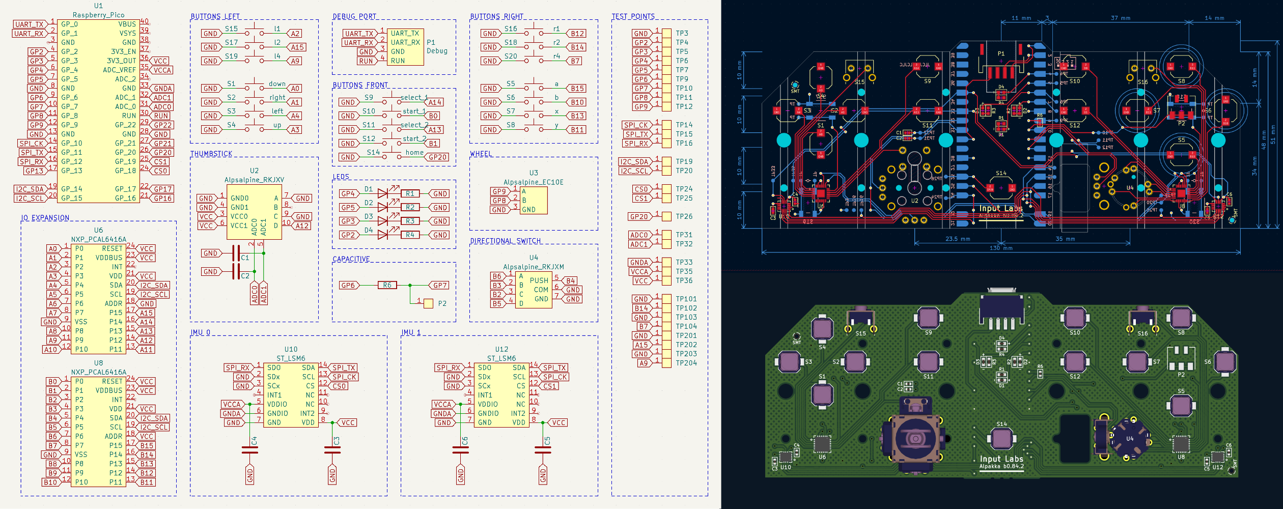
Main components on the Alpakka
Alpakka bill of materials (BOM)
61 components, 33 distinct parts.
| Qty | Part | Footprint | Refs |
|---|---|---|---|
| 2 | Alpsalpine_RKJXV | Alpsalpine_RKJXV122400R | U1, U2 |
| 1 | Alpsalpine_EC10E | Alpsalpine_EC10E | U3 |
| 2 | NXP_PCAL6416A | QFN24 | U6, U8 |
| 2 | ST_LSM6 | LGA14 | U10, U12 |
| 2 | Conn_01x20_Pin | Hirose_DF12NB_receptacle | P1, P2 |
| 1 | Conn_01x04 | XKB_X6511FRS-04 | P3 |
| 1 | Blade | HRO_BC-25-3P | P4 |
| 1 | Conn_01x02 | JST_PH_2_TH | P6 |
| 1 | down | Alpsalpine_SKPM | S1 |
| 1 | right | Alpsalpine_SKPM | S2 |
| 1 | left | Alpsalpine_SKPM | S3 |
| 1 | up | Alpsalpine_SKPM | S4 |
| 1 | A | Alpsalpine_SKPM | S5 |
| 1 | B | Alpsalpine_SKPM | S6 |
| 1 | X | Alpsalpine_SKPM | S7 |
| 1 | Y | Alpsalpine_SKPM | S8 |
| 1 | select_1 | Alpsalpine_SKPM | S9 |
| 1 | start_1 | Alpsalpine_SKPM | S10 |
| 1 | select_2 | Alpsalpine_SKPM | S11 |
| 1 | start_2 | Alpsalpine_SKPM | S12 |
Show 13 more
| Qty | Part | Footprint | Refs |
|---|---|---|---|
| 1 | home | Alpsalpine_SKPM | S14 |
| 1 | L1 | Alpsalpine_SKHHL | S15 |
| 1 | R1 | Alpsalpine_SKHHL | S16 |
| 1 | L2 | Alpsalpine_SKQG | S17 |
| 1 | R2 | Alpsalpine_SKQG | S18 |
| 1 | L4 | Alpsalpine_SKQG | S19 |
| 1 | R4 | Alpsalpine_SKQG | S20 |
| 8 | Endpoint | Pad_1mm | TP101, TP102, TP103, TP104, TP201, TP202, TP203, TP204 |
| 9 | Endpoint | Pad_1mm | TPA0, TPA1, TPA2, TPA3, TPBAT0, TPP0, TPP1, TPS0 +1 |
| 4 | Diode | 0603_d | D1, D2, D3, D4 |
| 4 | 100nF | 0402 | C1, C2, C3, C4 |
| 4 | 20 Ω | 0603 | R1, R2, R3, R4 |
| 1 | 1 MΩ | 0402 | R6 |
Alpakka design files
The KiCad project lives in the inputlabs/pcb repository on GitHub; these links point at the commit this page was built from.
Alpakka: common questions
How big is the Alpakka PCB?
The Alpakka measures 130 × 61 mm, has 2 copper layers and is 1.6 mm thick.
How many components are on the Alpakka?
61 components, from 33 distinct parts. The full bill of materials is listed on this page.
Where can I download the Alpakka design files?
From the inputlabs/pcb repository on GitHub, which has the KiCad layout and the schematic; the links under Design files point to each one.
Can I use the Alpakka design in my own project?
It is published under Custom license, which limits how it may be reused; read the license before building on it.