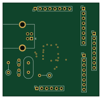
Kicad ci test

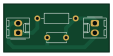
About the Kicad ci test PCB
Kicad ci test is an open source PCB design by INTI-CMNB, published on GitHub under the BSD-3-Clause license. It is a 2-layer board measuring 27.9 × 12.7 mm, with 4 components from 3 distinct parts.
By type, the board carries 2 connectors, 1 capacitor and 1 resistor.
From the project
Test for Continuous Integration using KiCad
Test for Continuous Integration using KiCad.
This repo contains two examples, one is the simplest situation and the other complicates things a little bit.
This is an example of how to test and generate documentation for a KiCad project automatically every time you commit a change to the schematic and/or PCB.
In this example we use a docker image containing KiCad, KiBot and all the supporting tools.
Kicad ci test bill of materials (BOM)
4 components, 3 distinct parts.
| Qty | Part | Footprint | Refs |
|---|---|---|---|
| 2 | Conn_01x02_Socket | Molex_KK-254_AE-6410-02A_1x02_P2.54mm_Vertical | J1, J2 |
| 1 | 1 uF | C_Disc_D5.0mm_W2.5mm_P5.00mm | C1 |
| 1 | 100 | R_Axial_DIN0207_L6.3mm_D2.5mm_P10.16mm_Horizontal | R1 |
Kicad ci test design files
The KiCad project lives in the INTI-CMNB/kicad_ci_test repository on GitHub; these links point at the commit this page was built from.
- Layoutkicad_ci_test.kicad_pcb
- Schematickicad_ci_test.kicad_sch
Kicad ci test: common questions
How big is the Kicad ci test PCB?
The Kicad ci test measures 27.9 × 12.7 mm, has 2 copper layers and is 1.6 mm thick.
How many components are on the Kicad ci test?
4 components, from 3 distinct parts. The full bill of materials is listed on this page.
Where can I download the Kicad ci test design files?
From the INTI-CMNB/kicad_ci_test repository on GitHub, which has the KiCad layout and the schematic; the links under Design files point to each one.
Can I use the Kicad ci test design in my own project?
Yes, under the terms of its BSD-3-Clause license, which INTI-CMNB chose for the repository.