
PCBEj1

About the PCBEj1 PCB
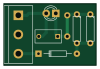
PCBEj1 is an open source PCB design by INTI-CMNB, published on GitHub. It is a 2-layer board measuring 24.4 × 16.3 mm, with 6 components from 5 distinct parts.
By type, the board carries 2 diodes, 2 resistors, 1 relay and 1 capacitor.
From the project
Prácticas para el curso Introductorio de de Kicad dictado por INTI
PCBEj1 bill of materials (BOM)
6 components, 5 distinct parts.
| Qty | Part | Footprint | Refs |
|---|---|---|---|
| 1 | CONN_3 | bornier3 | K1 |
| 1 | 1N4148 | Diode_DO-35_SOD27_Horizontal_RM10 | D1 |
| 1 | LED ROJO | LED-3MM | D2 |
| 1 | 100nF | C_Rect_L7_W3.5_P5 | C1 |
| 2 | 100K | R3-LARGE_PADS | R1, R2 |
PCBEj1 design files
The KiCad project lives in the INTI-CMNB/Practicas-Curso-Kicad repository on GitHub; these links point at the commit this page was built from.
PCBEj1: common questions
How big is the PCBEj1 PCB?
The PCBEj1 measures 24.4 × 16.3 mm, has 2 copper layers and is 1.6 mm thick.
How many components are on the PCBEj1?
6 components, from 5 distinct parts. The full bill of materials is listed on this page.
Where can I download the PCBEj1 design files?
From the INTI-CMNB/Practicas-Curso-Kicad repository on GitHub, which has the KiCad layout; the links under Design files point to each one.
Can I use the PCBEj1 design in my own project?
The repository has no license, so all rights stay with INTI-CMNB. Use it as a reference, and ask the author before reusing the design.
More boards in Practicas-Curso-Kicad
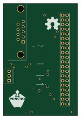
Salguero Federico2
40.6 × 61 mm13 partsNo license2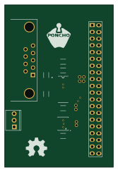
Ejercicio 2 - Santiago Nolasco
40.6 × 61 mm13 partsNo license2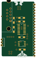
Ejercicio 2
29.2 × 48.8 mm13 parts2LNo license2
Nolasco Santiago
24.1 × 17 mm6 parts2LNo license2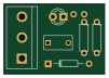
Sebastiansisevich
24.8 × 17.1 mm6 parts2LNo license2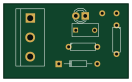
Escobar Martin
33 × 19.7 mm6 parts2LNo license2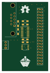
Ejercicio2
40.6 × 61 mm6 parts2LNo license2
Ejercicio 1
24.1 × 17.8 mm6 parts2LNo license2
Pcb ej1
24.1 × 17.2 mm6 parts2LNo license2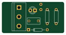
Salguero Federico
33.5 × 17 mm6 parts2LNo license2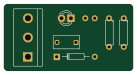
Dia1 Ejercisio1
34.3 × 17.8 mm6 parts2LNo license2