
FPGA1394V3-IO

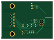
About the FPGA1394V3-IO PCB
FPGA1394V3-IO is an open source PCB design by jhu-cisst, published on GitHub. It is a 2-layer board measuring 45.7 × 33 mm, with 14 components from 10 distinct parts.
Other key parts include the MIC2091-1YM5 and SMS3.3.TCT. By type, the board carries 5 resistors, 4 capacitors, 2 ICs, 2 connectors and 1 diode.
From the project
PCB Design for I/O board used with FPGA1394V3
PCB design for I/O board used with FPGA1394V3, in KiCad format.
This board connects to the DF11 connector (J9) on FPGA1394V3, which provides +3.3V, GND and 4 I/O signals (MIO34-37) from the Zynq SoC PS, and makes protected versions of these signals available on a DB9F connector. Specifically, the +3.3V output has a 100 mA current limit and the I/O signals have 50 Ohm current-limiting resistors and a transorb (TVS diode) for protection.
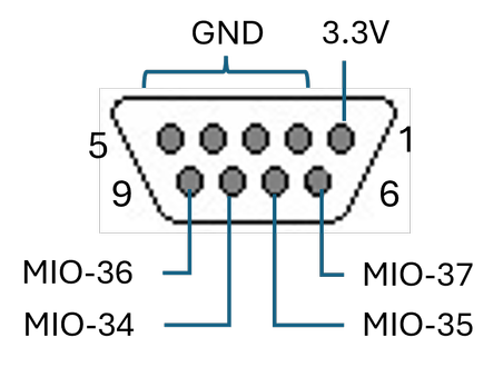
Main components on the FPGA1394V3-IO
FPGA1394V3-IO bill of materials (BOM)
14 components, 10 distinct parts — part numbers from the project's BOM.
| Qty | Part | Footprint | Refs |
|---|---|---|---|
| 1 | MIC2091-1YM5 MIC2091-1YM5-TR Microchip | SOT-23-5_M5_MCH | U1 |
| 1 | SMS3.3.TCT Semtech | SOT95P280X145-6N | U2 |
| 1 | 622-009-260-033 DB9F EDAC | 6E17C009SBF220 | J1 |
| 1 | Hirose DF11 Hirose | SHDRRA6W60P200X200_2X3_800X1000X530P | J2 |
| 1 | LED Generic | LED_LSM0805-2P0X1P25X0P8_VCC | D1 |
| 1 | C1608X7R1C105KT000N 1uF TDK | C_0603_1608Metric | C1 |
| 2 | GRM188C81C106MA73D 10uF Murata | C_0603_1608Metric | C2, C3 |
| 1 | C0603C104K4RACTU 0.1uF Kemet | C_0603_1608Metric | C4 |
| 4 | CRCW060350R0FKEA 50 Vishay Dale | R_0603_1608Metric | R1, R2, R3, R4 |
| 1 | 499 Generic | R_0603_1608Metric | R5 |
FPGA1394V3-IO design files
The KiCad project lives in the jhu-cisst/FPGA1394V3-IO-PCB repository on GitHub; these links point at the commit this page was built from.
- Layoutdvrk-ios.kicad_pcb
- Schematicdvrk-ios.kicad_sch
- BOMdvrk-ios-bom.xlsx
FPGA1394V3-IO: common questions
How big is the FPGA1394V3-IO PCB?
The FPGA1394V3-IO measures 45.7 × 33 mm, has 2 copper layers and is 1.6 mm thick.
How many components are on the FPGA1394V3-IO?
14 components, from 10 distinct parts, with part numbers taken from the project's own BOM. The full bill of materials is listed on this page.
Where can I download the FPGA1394V3-IO design files?
From the jhu-cisst/FPGA1394V3-IO-PCB repository on GitHub, which has the KiCad layout, the schematic and the BOM; the links under Design files point to each one.
Can I use the FPGA1394V3-IO design in my own project?
The repository has no license, so all rights stay with jhu-cisst. Use it as a reference, and ask the author before reusing the design.