
Elements

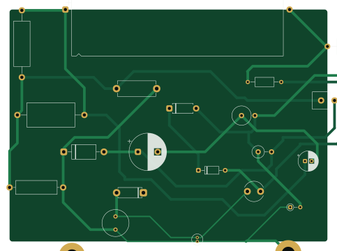
About the Elements PCB
Elements is an open source PCB design by KamMalinski, published on GitHub under the AGPL-3.0 license. It is a 2-layer board measuring 120.5 × 88 mm, with 20 components from 20 distinct parts.
By type, the board carries 5 diodes, 5 inductors, 5 capacitors and 5 resistors.
From the project
Automatic PCB Analysis and Reverse Engineering
This directory contains a curated test dataset of small PCB examples used for evaluating PCB image analysis and schematic reconstruction workflows.
- two raster images of the PCB, one for the top side and one for the bottom side; - a KiCad project directory with the reference PCB and schematic files.
The dataset is organized by sample name:
The raster images are PNG files. They should be interpreted as pixel images of the PCB sides:
Elements bill of materials (BOM)
20 components, 20 distinct parts.
| Qty | Part | Footprint | Refs |
|---|---|---|---|
| 1 | D | D_5W_P10.16mm_Horizontal | D1 |
| 1 | D | D_A-405_P10.16mm_Horizontal | D2 |
| 1 | D | D_DO-15_P10.16mm_Horizontal | D3 |
| 1 | D | D_DO-35_SOD27_P3.81mm_Vertical_AnodeUp | D4 |
| 1 | D | D_DO-201AE_P15.24mm_Horizontal | D5 |
| 1 | 1uH | L_Radial_D7.5mm_P5.00mm_Fastron_07P | L1 |
| 1 | 10mH | L_Axial_L7.0mm_D3.3mm_P12.70mm_Horizontal_Fastron_MICC | L2 |
| 1 | 4.7mH | L_Axial_L12.8mm_D5.8mm_P20.32mm_Horizontal_Fastron_HBCC | L3 |
| 1 | 22mH | L_Axial_L24.0mm_D7.1mm_P5.08mm_Vertical_Vishay_IM-10-28 | L4 |
| 1 | 100mH | L_Axial_L14.0mm_D4.5mm_P5.08mm_Vertical_Fastron_LACC | L5 |
| 1 | 10uF | C_Radial_D4.0mm_H5.0mm_P1.50mm | C1 |
| 1 | 100uF | C_Radial_D10.0mm_H16.0mm_P5.00mm | C2 |
| 1 | 2.2uF | CP_Axial_L80.0mm_D35.0mm_P85.00mm_Horizontal | C3 |
| 1 | 220uF | CP_Radial_D7.5mm_P2.50mm | C4 |
| 1 | 100uF | CP_Radial_D14.0mm_P7.50mm | C5 |
| 1 | 10R | R_Axial_DIN0516_L15.5mm_D5.0mm_P20.32mm_Horizontal | R1 |
| 1 | 22R | R_Axial_DIN0614_L14.3mm_D5.7mm_P15.24mm_Horizontal | R2 |
| 1 | 1K | R_Axial_DIN0617_L17.0mm_D6.0mm_P25.40mm_Horizontal | R3 |
| 1 | 470R | R_Axial_DIN0918_L18.0mm_D9.0mm_P25.40mm_Horizontal | R4 |
| 1 | 10K | R_Axial_Power_L20.0mm_W6.4mm_P5.08mm_Vertical | R5 |
Elements design files
The KiCad project lives in the KamMalinski/PRISM repository on GitHub; these links point at the commit this page was built from.
Elements: common questions
How big is the Elements PCB?
The Elements measures 120.5 × 88 mm, has 2 copper layers and is 1.6 mm thick.
How many components are on the Elements?
20 components, from 20 distinct parts. The full bill of materials is listed on this page.
Where can I download the Elements design files?
From the KamMalinski/PRISM repository on GitHub, which has the KiCad layout and the schematic; the links under Design files point to each one.
Can I use the Elements design in my own project?
Yes, under the terms of its AGPL-3.0 license, which KamMalinski chose for the repository.
More boards in PRISM
Cascade
26.5 × 68.5 mm19 parts2LAGPL-3.03
Filter
55.1 × 40 mm7 parts2LAGPL-3.03
Connector
47.7 × 49 mm6 parts2LAGPL-3.03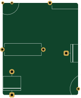
Crossover
41.3 × 50.4 mm6 parts2LAGPL-3.03
Transistors
14.3 × 21.1 mm5 parts2LAGPL-3.03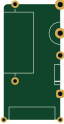
Round
15 × 30.7 mm4 parts2LAGPL-3.03
Divider
53 × 8 mm4 parts2LAGPL-3.03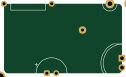
Floating
31.4 × 18.5 mm4 parts2LAGPL-3.03
Groundplane
18.5 × 37.9 mm4 parts2LAGPL-3.03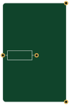
Meander
23.8 × 36.9 mm3 parts2LAGPL-3.03