
Filter

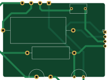
About the Filter PCB
Filter is an open source PCB design by KamMalinski, published on GitHub under the AGPL-3.0 license. It is a 2-layer board measuring 55.1 × 40 mm, with 7 components from 7 distinct parts.
By type, the board carries 2 connectors, 2 inductors, 2 capacitors and 1 resistor.
From the project
Automatic PCB Analysis and Reverse Engineering
This directory contains a curated test dataset of small PCB examples used for evaluating PCB image analysis and schematic reconstruction workflows.
- two raster images of the PCB, one for the top side and one for the bottom side; - a KiCad project directory with the reference PCB and schematic files.
The dataset is organized by sample name:
The raster images are PNG files. They should be interpreted as pixel images of the PCB sides:
Filter bill of materials (BOM)
7 components, 7 distinct parts.
| Qty | Part | Footprint | Refs |
|---|---|---|---|
| 1 | Conn_01x04 | SolderWire-0.5sqmm_1x04_P4.8mm_D0.9mm_OD2.3mm | J1 |
| 1 | Conn_01x04 | PinHeader_1x04_P2.54mm_Horizontal | J2 |
| 1 | 20nH | L_Axial_L20.0mm_D8.0mm_P7.62mm_Vertical | L1 |
| 1 | 330mH | L_Axial_L29.9mm_D14.0mm_P38.00mm_Horizontal_Vishay_IHA-105 | L2 |
| 1 | 20mF | CP_Radial_Tantal_D8.0mm_P5.00mm | C1 |
| 1 | 470pF | C_Rect_L9.0mm_W4.9mm_P7.50mm_MKT | C2 |
| 1 | 100R | R_Axial_Power_L20.0mm_W6.4mm_P25.40mm | R1 |
Filter design files
The KiCad project lives in the KamMalinski/PRISM repository on GitHub; these links point at the commit this page was built from.
Filter: common questions
How big is the Filter PCB?
The Filter measures 55.1 × 40 mm, has 2 copper layers and is 1.6 mm thick.
How many components are on the Filter?
7 components, from 7 distinct parts. The full bill of materials is listed on this page.
Where can I download the Filter design files?
From the KamMalinski/PRISM repository on GitHub, which has the KiCad layout and the schematic; the links under Design files point to each one.
Can I use the Filter design in my own project?
Yes, under the terms of its AGPL-3.0 license, which KamMalinski chose for the repository.
More boards in PRISM
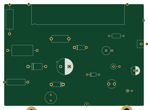
Elements
120.5 × 88 mm20 parts2LAGPL-3.03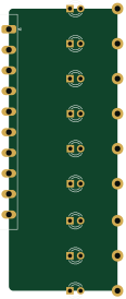
Cascade
26.5 × 68.5 mm19 parts2LAGPL-3.03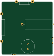
Connector
47.7 × 49 mm6 parts2LAGPL-3.03
Crossover
41.3 × 50.4 mm6 parts2LAGPL-3.03
Transistors
14.3 × 21.1 mm5 parts2LAGPL-3.03
Round
15 × 30.7 mm4 parts2LAGPL-3.03
Divider
53 × 8 mm4 parts2LAGPL-3.03
Floating
31.4 × 18.5 mm4 parts2LAGPL-3.03
Groundplane
18.5 × 37.9 mm4 parts2LAGPL-3.03
Meander
23.8 × 36.9 mm3 parts2LAGPL-3.03