
Ledger nano x pads

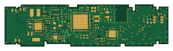
About the Ledger nano x pads PCB
Ledger nano x pads is an open source STM32 PCB design by KarpelesLab, published on GitHub under the CC-BY-4.0 license. It is a 4-layer board measuring 61.7 × 15.9 mm, with 137 components from 59 distinct parts.
Its main chip is the STM32WB35CCU6A, from the STM32 family. By type, the board carries 40 test points, 34 resistors, 33 capacitors, 11 crystals, 5 connectors and 2 switches.
From the project
Interactive map of the Ledger Nano X main board: test pads, traced nets and a KiCad reconstruction with 2D photo and 3D viewers
An interactive map of the Ledger Nano X main board: its 40 test pads, the copper traces between them and the chips, and a KiCad reconstruction of the whole board.
View it online: https://karpeleslab.github.io/ledgernanoxpads/**
- Photo viewer: photos of both sides, with and without components, overlaid with every traced net, test pad and part; hover anything for details. - 3D viewer: the KiCad reconstruction with every part and its marking; hover a track, pad or chip to light up its net.
Main components on the Ledger nano x pads
Ledger nano x pads bill of materials (BOM)
137 components, 59 distinct parts.
| Qty | Part | Footprint | Refs |
|---|---|---|---|
| 1 | STM32WB35CCU6A | MCU1 | |
| 6 | ? | X1, X4, X5, X6, X7, X8 | |
| 1 | unknown, marked 2GC | X2 | |
| 1 | unknown, marked 6 | X3 | |
| 1 | unknown, marked P8W 26 | X9 | |
| 1 | unknown, marked 1C4F, likely a switching regulator for the +3.3V rail | X10 | |
| 1 | crystal, likely the 32 MHz HSE | Y1 | |
| 5 | likely an ESD protection diode, marked P | P1, P2, P3, P4, P5 | |
| 1 | chip antenna | ANT1 | |
| 1 | battery contacts | BAT1 | |
| 1 | Hirose BM20B(0.8)-16DS-0.4V(51) | BTB1 | |
| 3 | unknown | PWR1, PWR2, PWR3 | |
| 1 | RF filter / matching device | RFF1 | |
| 1 | secure element | SE1 | |
| 1 | push button, left | SW1 | |
| 1 | push button, right | SW2 | |
| 1 | USB CC2 | TP01 | |
| 2 | Left button power | TP02, TP19 | |
| 2 | TestPoint | TP03, TP08 | |
| 1 | MCU PB7 | TP04 |
Show 39 more
| Qty | Part | Footprint | Refs |
|---|---|---|---|
| 1 | PD SCL | TP05 | |
| 1 | BAT NTC? | TP06 | |
| 1 | Switched supply? | TP07 | |
| 1 | PD SDA | TP09 | |
| 1 | I2C1 SCL | TP10 | |
| 1 | PD VBUS_EN_SNK | TP11 | |
| 1 | VBUS | TP12 | |
| 1 | PWR1 pin 12 | TP13 | |
| 1 | VBAT? | TP14 | |
| 1 | PWR1 to MCU PA2? | TP15 | |
| 1 | MCU PB3 | TP16 | |
| 1 | I2C1 SDA | TP17 | |
| 1 | PWR1 pin 15 | TP18 | |
| 1 | SWCLK | TP20 | |
| 1 | SWDIO | TP21 | |
| 1 | Supply sense (MCU PA1) | TP22 | |
| 1 | GND | TP23 | |
| 1 | +3.3V rail | TP24 | |
| 1 | MCU PA5 | TP25 | |
| 1 | MCU NRST | TP26 | |
| 1 | MCU PA7 | TP27 | |
| 1 | Left button | TP28 | |
| 1 | SE RESET | TP29 | |
| 1 | SE CLK-IN | TP30 | |
| 1 | OLED SPI CS | TP31 | |
| 1 | SEPROXYHAL | TP32 | |
| 1 | OLED RESET? | TP33 | |
| 1 | OLED CLK | TP34 | |
| 1 | OLED MOSI | TP35 | |
| 1 | OLED D/C | TP36 | |
| 1 | BTB pin 9 | TP37 | |
| 1 | Regulator input? | TP38 | |
| 1 | OLED IREF? | TP39 | |
| 1 | Right button | TP40 | |
| 1 | USB-C receptacle | USB1 | |
| 1 | STUSB4500L | USBPD1 | |
| 1 | unknown, likely a shielded power inductor | L1 | |
| 33 | C | C1, C2, C3, C5, C6, C7, C8, C9 +25 | |
| 34 | R | R1, R3, R4, R5, R6, R7, R8, R9 +26 |
Ledger nano x pads design files
The KiCad project lives in the KarpelesLab/ledger_nano_x_pads repository on GitHub; these links point at the commit this page was built from.
- Layoutkicad/nanox.kicad_pcb
- Schematickicad/nanox.kicad_sch
Ledger nano x pads: common questions
What microcontroller does the Ledger nano x pads use?
The Ledger nano x pads is built around the STM32WB35CCU6A, from the STM32 family.
How big is the Ledger nano x pads PCB?
The Ledger nano x pads measures 61.7 × 15.9 mm, has 4 copper layers and is 0.6 mm thick.
How many components are on the Ledger nano x pads?
137 components, from 59 distinct parts. The full bill of materials is listed on this page.
Where can I download the Ledger nano x pads design files?
From the KarpelesLab/ledger_nano_x_pads repository on GitHub, which has the KiCad layout and the schematic; the links under Design files point to each one.
Can I use the Ledger nano x pads design in my own project?
Yes, under the terms of its CC-BY-4.0 license, which KarpelesLab chose for the repository.
Can I test firmware for the Ledger nano x pads without the hardware?
Yes. HardLabs builds a simulation of the board from its netlist and BOM, so you can run and debug STM32 firmware against it before you order a PCB.
Similar boards
 STM32
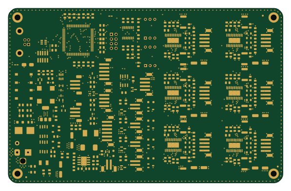
LumenPnP Motherboard
opulo-inc
149 × 95 mm296 parts4LCC-BY-SA-4.03.7k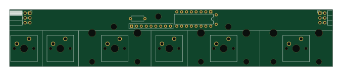 STM32
Type g
google
169 × 30 mm24 parts2LApache-2.02.9k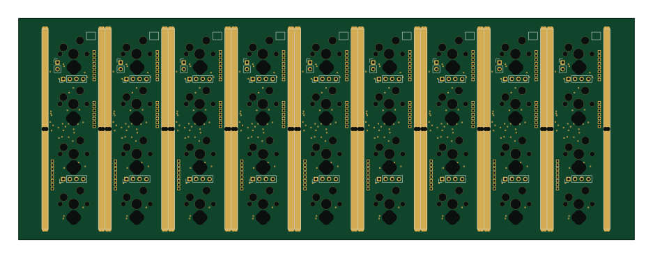 STM32
Main panel
234 × 84 mm26 parts4LApache-2.02.9k STM32
Base
52.3 × 52.3 mm36 parts2LApache-2.02.9k STM32
Type a
150 × 30 mm14 parts2LApache-2.02.9k STM32
Type c
188 × 30 mm17 parts2LApache-2.02.9k