Isense


About the Isense PCB
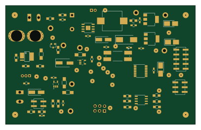
Isense is an open source PCB design by kloper, published on GitHub under the GPL-2.0 license. It is a 2-layer board measuring 20.3 × 15.2 mm, with 11 components from 6 distinct parts.
Other key parts include the OPA237NA_250. By type, the board carries 7 resistors, 3 ICs and 1 connector.
From the project
My take on HAKKO T12 tips soldering station
I am working on my own soldering station based on HAKKO T12 cartriges. Electronics is related to the one found on EEVBlog forum https://www.eevblog.com/forum/reviews/t12-stm32-v2-1s-soldering-station-controller-schematic-etc/
Firmware will be built from scratch. Work in progress.
Main components on the Isense
Isense bill of materials (BOM)
11 components, 6 distinct parts.
| Qty | Part | Footprint | Refs |
|---|---|---|---|
| 3 | OPA237NA_250 | SOT95P280X145-5N | U1, U2, U3 |
| 1 | IN | Pin_Header_Straight_1x04_Pitch2.54mm | J1 |
| 2 | 7.5K | R_0805_HandSoldering | R1, R2 |
| 2 | 20K | R_0805_HandSoldering | R3, R4 |
| 2 | 470K | R_1206_HandSoldering | R5, R6 |
| 1 | 100K | R_0805_2012Metric_Pad1.20x1.40mm_HandSolder | R7 |
Isense design files
The KiCad project lives in the kloper/st12 repository on GitHub; these links point at the commit this page was built from.
Isense: common questions
How big is the Isense PCB?
The Isense measures 20.3 × 15.2 mm, has 2 copper layers and is 1.6 mm thick.
How many components are on the Isense?
11 components, from 6 distinct parts. The full bill of materials is listed on this page.
Where can I download the Isense design files?
From the kloper/st12 repository on GitHub, which has the KiCad layout; the links under Design files point to each one.
Can I use the Isense design in my own project?
Yes, under the terms of its GPL-2.0 license, which kloper chose for the repository.