
Electroscope through

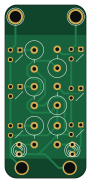
About the Electroscope through PCB
Electroscope through is an open source PCB design by konspyre, published on GitHub. It is a 2-layer board measuring 21.3 × 45.7 mm, with 17 components from 8 distinct parts.
Other key parts include the ANT. By type, the board carries 6 transistors, 6 resistors, 2 ICs, 2 diodes and 1 battery holder.
From the project
electroscope with through-hole parts
This is a similar board to the surface mount electroscope but is easier (or harder, depending on your manufacturing viewpoint) to assemble and source parts for.
This BOM specifies the amount needed for one board. Parts have been translated from their surface mount equivalents.
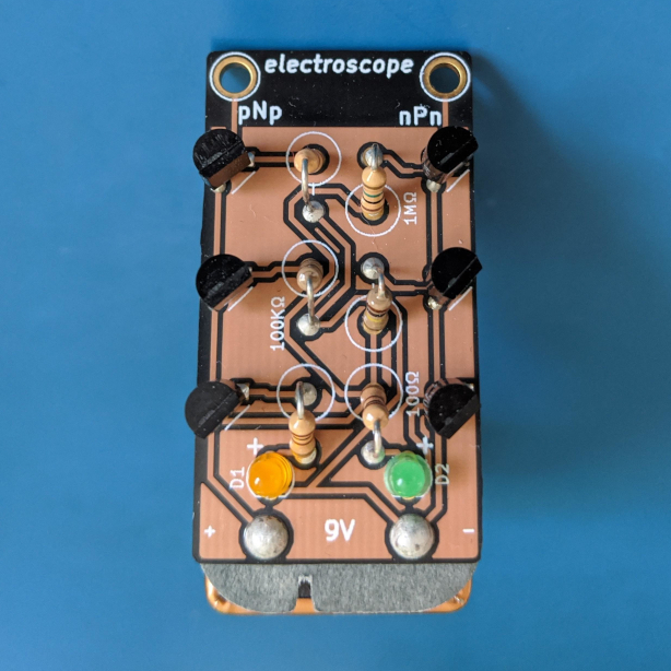
Main components on the Electroscope through
Electroscope through bill of materials (BOM)
17 components, 8 distinct parts.
| Qty | Part | Footprint | Refs |
|---|---|---|---|
| 2 | ANT | 1pin | U1, U2 |
| 3 | Q_PNP_EBC | TO92-123 | Q1, Q3, Q5 |
| 3 | Q_NPN_EBC | TO92-123 | Q2, Q4, Q6 |
| 1 | Battery | 9VBATT_TH | BT1 |
| 2 | LED | LED-3MM | D1, D2 |
| 2 | 100Ω | Resistor_Vertical_RM5mm | R1, R6 |
| 2 | 1MΩ | Resistor_Vertical_RM5mm | R2, R5 |
| 2 | 100KΩ | Resistor_Vertical_RM5mm | R3, R4 |
Electroscope through design files
The KiCad project lives in the konspyre/electroscope-through repository on GitHub; these links point at the commit this page was built from.
Electroscope through: common questions
How big is the Electroscope through PCB?
The Electroscope through measures 21.3 × 45.7 mm, has 2 copper layers and is 1.6 mm thick.
How many components are on the Electroscope through?
17 components, from 8 distinct parts. The full bill of materials is listed on this page.
Where can I download the Electroscope through design files?
From the konspyre/electroscope-through repository on GitHub, which has the KiCad layout; the links under Design files point to each one.
Can I use the Electroscope through design in my own project?
The repository has no license, so all rights stay with konspyre. Use it as a reference, and ask the author before reusing the design.