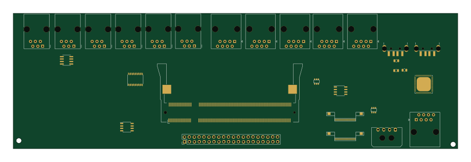
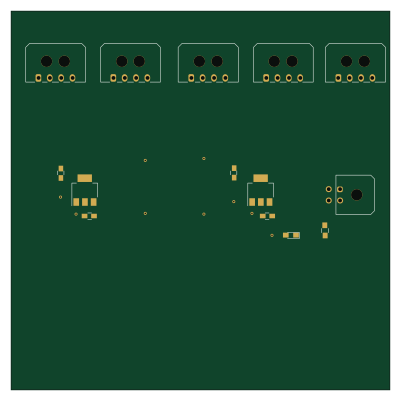
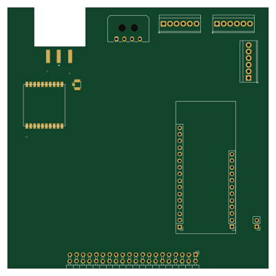
CyBack

About the CyBack PCB
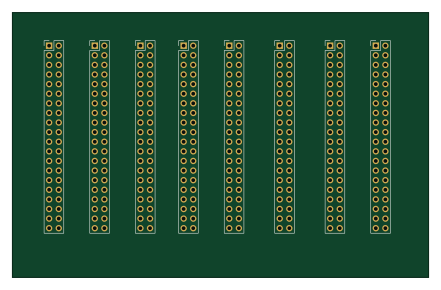
CyBack is an open source PCB design by M2I-HABET, published on GitHub. It is a 2-layer board measuring 110 × 70 mm, with 8 components from 1 distinct parts.
From the project
This is the electronics stack and associated software for a module payload stack
CyBack bill of materials (BOM)
8 components, 1 distinct parts.
| Qty | Part | Footprint | Refs |
|---|---|---|---|
| 8 | Conn_02x20_Odd_Even | Pin_Header_Straight_2x20_Pitch2.54mm | J1, J2, J3, J4, J5, J6, J7, J8 |
CyBack design files
The KiCad project lives in the M2I-HABET/CyStack repository on GitHub; these links point at the commit this page was built from.
CyBack: common questions
How big is the CyBack PCB?
The CyBack measures 110 × 70 mm, has 2 copper layers and is 1.6 mm thick.
How many components are on the CyBack?
8 components, from 1 distinct parts. The full bill of materials is listed on this page.
Where can I download the CyBack design files?
From the M2I-HABET/CyStack repository on GitHub, which has the KiCad layout; the links under Design files point to each one.
Can I use the CyBack design in my own project?
The repository has no license, so all rights stay with M2I-HABET. Use it as a reference, and ask the author before reusing the design.