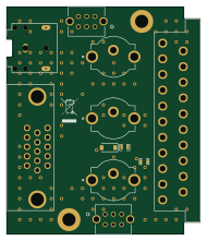
Panel

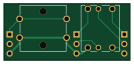
About the Panel PCB
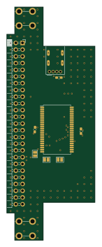
Panel is an open source PCB design by marqs85, published on GitHub under the CERN-OHL-P-2.0 license. It is a 2-layer board measuring 33.5 × 15 mm, with 5 components from 3 distinct parts.
By type, the board carries 3 connectors and 2 switches.
From the project
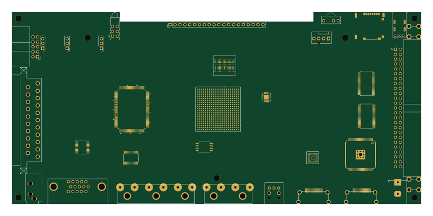
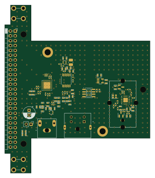
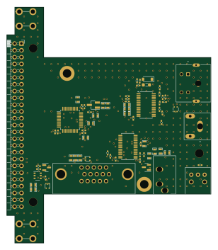
OSSC Pro HW files
This repository is a collection of various files for OSSC Pro board, related adapters and expansion cards. Unless otherwise mentioned, designs listed below are work in progress and not guaranteed to be production quality. Use at your own risk.
Contents --------------------------------------------------- OSSC Pro PCB (free version) Schematic is complete and matches production version 1.6 Connector placement is complete and matches production version 1.6 BOM is complete and matches production version 1.6 * Placement of the components and routing are incomplete
Panel bill of materials (BOM)
5 components, 3 distinct parts.
| Qty | Part | Footprint | Refs |
|---|---|---|---|
| 3 | TSW-101-08-T-T-RA | PinHeader_1x03_P2.54mm_Vertical | J1, J2, J3 |
| 1 | SKQUCAA010 | SKQUCAA010 | SW1 |
| 1 | B3F-4050 | B3F-4050 | SW2 |
Panel design files
The KiCad project lives in the marqs85/ossc_pro_hw repository on GitHub; these links point at the commit this page was built from.
Panel: common questions
How big is the Panel PCB?
The Panel measures 33.5 × 15 mm, has 2 copper layers and is 1.6 mm thick.
How many components are on the Panel?
5 components, from 3 distinct parts. The full bill of materials is listed on this page.
Where can I download the Panel design files?
From the marqs85/ossc_pro_hw repository on GitHub, which has the KiCad layout; the links under Design files point to each one.
Can I use the Panel design in my own project?
Yes, under the terms of its CERN-OHL-P-2.0 license, which marqs85 chose for the repository.