
LAYR

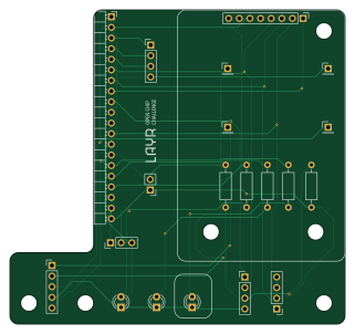
About the LAYR PCB
LAYR is an open source PCB design by OCDCpro, published on GitHub under the CC-BY-4.0 license. It is a 2-layer board measuring 80 × 75 mm, with 20 components from 14 distinct parts.
By type, the board carries 12 connectors, 5 resistors and 3 diodes.
From the project
The LAYR files.
The components of the LAYR hardware kit are used in the demonstrator to assemble a doorlock.

LAYR bill of materials (BOM)
20 components, 14 distinct parts.
| Qty | Part | Footprint | Refs |
|---|---|---|---|
| 1 | +12V | PinHeader_1x01_P2.54mm_Vertical | J1 |
| 1 | to_ULX3S | PinHeader_1x20_P2.54mm_Horizontal | J2 |
| 1 | GND_from_12V | PinHeader_1x01_P2.54mm_Vertical | J3 |
| 1 | +5V | PinHeader_1x01_P2.54mm_Vertical | J4 |
| 1 | GND | PinHeader_1x01_P2.54mm_Vertical | J5 |
| 1 | to_lock | PinHeader_1x05_P2.54mm_Vertical | J6 |
| 1 | mem_1-4 | PinHeader_1x04_P2.54mm_Vertical | J7 |
| 1 | mem_5-8 | PinHeader_1x04_P2.54mm_Vertical | J8 |
| 1 | to_RC522 | PinHeader_1x08_P2.54mm_Vertical | J9 |
| 1 | to_uart | PinHeader_1x04_P2.54mm_Vertical | J10 |
| 1 | rst_button | PinHeader_1x02_P2.54mm_Vertical | J11 |
| 1 | mode_switch | PinHeader_1x03_P2.54mm_Vertical | J12 |
| 3 | LED | LED_D3.0mm | D1, D2, D3 |
| 5 | 4K7 | R_Axial_DIN0207_L6.3mm_D2.5mm_P10.16mm_Horizontal | R1, R2, R3, R4, R5 |
LAYR design files
The KiCad project lives in the OCDCpro/LAYR repository on GitHub; these links point at the commit this page was built from.
LAYR: common questions
How big is the LAYR PCB?
The LAYR measures 80 × 75 mm, has 2 copper layers and is 1.6 mm thick.
How many components are on the LAYR?
20 components, from 14 distinct parts. The full bill of materials is listed on this page.
Where can I download the LAYR design files?
From the OCDCpro/LAYR repository on GitHub, which has the KiCad layout and the schematic; the links under Design files point to each one.
Can I use the LAYR design in my own project?
Yes, under the terms of its CC-BY-4.0 license, which OCDCpro chose for the repository.