
Dsi hb-1.3-reverse engineering

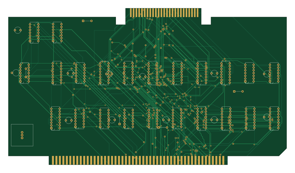
About the Dsi hb-1.3-reverse engineering PCB
Dsi hb-1.3-reverse engineering is an open source PCB design by peclark1, published on GitHub. It is a 2-layer board measuring 254 × 143 mm, with 30 components from 15 distinct parts.
Other key parts include the 74367, 7405, 7410, 7400 and 7420. By type, the board carries 10 modules, 2 connectors and 2 capacitors.
From the project
This package keeps the reconstructed HB-1.3 schematic and PCB in one KiCad project.
This package keeps the reconstructed HB-1.3 schematic and PCB in one KiCad project.
v0.9 completes the current reconstructed PCB netlist. The two signal joins left in v0.8 (NPHLDA and RBAR) are routed, and all 23 assigned IC +5V pads and all 23 assigned IC GND pads are joined into their respective trees.
Internal connectivity results for the final PCB:
- 2,867 track segments - 371 vias - 130 named electrical nets, plus net 0 - 0 split assigned nets - 0 remaining assigned-net tree joins
Main components on the Dsi hb-1.3-reverse engineering
Dsi hb-1.3-reverse engineering bill of materials (BOM)
30 components, 15 distinct parts.
| Qty | Part | Footprint | Refs |
|---|---|---|---|
| 5 | 74367 | DIP-16_W7.62mm | A1, A7, A8, A9, A10 |
| 2 | 7405 | DIP-14_W7.62mm | A2, A3 |
| 1 | 7410 | DIP-14_W7.62mm | A4 |
| 1 | 7400 | DIP-14_W7.62mm | A5 |
| 1 | 7420 | DIP-14_W7.62mm | A6 |
| 1 | S-100 EDGE 100 | S100_EDGE_100 | J1 |
| 1 | FDC-1 50-pin edge | FDC1_EDGE_50 | J2 |
| 1 | 7404 | DIP-14_W7.62mm | B1 |
| 7 | 74367 | DIP-16_W7.62mm | B2, B4, B5, B6, B7, B8, B9 |
| 2 | 7400 | DIP-14_W7.62mm | B3, B11 |
| 1 | 7405 | DIP-14_W7.62mm | B10 |
| 4 | PHOTO_PLACEHOLDER | AXIAL_P7.62 | D_PHYS1, R_PHYS1, R_PHYS2, R_PHYS3 |
| 1 | TO-220 regulator, exact part TBD | TO220_HEATSINK_PLACEHOLDER | VR_PHYS1 |
| 1 | 74164 | DIP-14_W7.62mm | C1 |
| 1 | 7402 | DIP-14_W7.62mm | C2 |
Dsi hb-1.3-reverse engineering design files
The KiCad project lives in the peclark1/dsi-hb-1.3-reverse-engineering repository on GitHub; these links point at the commit this page was built from.
Dsi hb-1.3-reverse engineering: common questions
How big is the Dsi hb-1.3-reverse engineering PCB?
The Dsi hb-1.3-reverse engineering measures 254 × 143 mm, has 2 copper layers and is 1.6 mm thick.
How many components are on the Dsi hb-1.3-reverse engineering?
30 components, from 15 distinct parts. The full bill of materials is listed on this page.
Where can I download the Dsi hb-1.3-reverse engineering design files?
From the peclark1/dsi-hb-1.3-reverse-engineering repository on GitHub, which has the KiCad layout; the links under Design files point to each one.
Can I use the Dsi hb-1.3-reverse engineering design in my own project?
The repository has no license, so all rights stay with peclark1. Use it as a reference, and ask the author before reusing the design.