
Kicad project

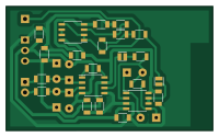
About the Kicad project PCB
Kicad project is an open source PCB design by Phelma-BE2, published on GitHub under the GPL-3.0 license. It is a 2-layer board measuring 50 × 30 mm, with 55 components from 18 distinct parts.
Other key parts include the AD620A, TL082 and LM311N. By type, the board carries 16 resistors, 12 capacitors, 10 diodes, 8 ICs, 5 relays and 2 jumpers.
From the project
kicad project for the BE, with simulation using ltspice ( nice waveforms ) or ngspice ( ++ foss )
launch the simulation (ltspice) ---------------------------------- - kicad have to be launched in the root of the project or else it will complain that sim/kicaltspice.sh cannot be found. - open be2.sch in eeschema you can modify/add spice commands in comments blocks beginning with +PSPICE. - then tools > generate netlist file > Spice tab, fill "simulator command" with sim/kicaltspice.sh and press "Run Simulator". Ltspice will immediately run the simulation and graph plots using the last saved plot configuration file be2.plt.
Main components on the Kicad project
Kicad project bill of materials (BOM)
55 components, 18 distinct parts.
| Qty | Part | Footprint | Refs |
|---|---|---|---|
| 1 | AD620A | SOIC-8_3.9x4.9mm_Pitch1.27mm | U1 |
| 3 | TL082 | SOIC-8_3.9x4.9mm_Pitch1.27mm | U2, U3, U4 |
| 4 | LM311N | SOIC-8_3.9x4.9mm_Pitch1.27mm | U100, U101, U102, U103 |
| 2 | jp_close | JP_20mil | JP1, JP2 |
| 2 | CONN_01X03 | Pin_Header_Straight_1x03_phelma | K1, K4 |
| 1 | CONN_01X02 | Pin_Header_Straight_1x02_phelma | K2 |
| 2 | CONN_01X01 | Pin_Header_Straight_1x01_phelma | K3, K5 |
| 2 | JP3 | JP_20mil | jp_close1, jp_close2 |
| 6 | 1n4148 | Diode_DO-41_SOD81_Vertical_AnodeUp_phelma | D1, D2, D3, D4, D5, D6 |
| 4 | LED | KP-3216SRC-PRV | D100, D101, D102, D103 |
| 2 | 1u | C_1206 | C1, C2 |
| 8 | 10n | C_1206 | C3, C4, C6, C7, C8, C10, C11, C12 |
| 2 | 330n | C_1206 | C5, C9 |
| 1 | 270k | R_1206 | R1 |
| 5 | 100K | R_1206 | R2, R3, R4, R5, R7 |
| 5 | 1k | R_1206 | R6, R100, R101, R102, R103 |
| 2 | 10K | R_1206 | R8, R9 |
| 3 | R_Small | R_1206 | R11, R12, R13 |
Kicad project design files
The KiCad project lives in the Phelma-BE2/kicad-project repository on GitHub; these links point at the commit this page was built from.
- Layoutbe2.kicad_pcb
Kicad project: common questions
How big is the Kicad project PCB?
The Kicad project measures 50 × 30 mm, has 2 copper layers and is 1.6 mm thick.
How many components are on the Kicad project?
55 components, from 18 distinct parts. The full bill of materials is listed on this page.
Where can I download the Kicad project design files?
From the Phelma-BE2/kicad-project repository on GitHub, which has the KiCad layout; the links under Design files point to each one.
Can I use the Kicad project design in my own project?
Yes, under the terms of its GPL-3.0 license, which Phelma-BE2 chose for the repository.