Projjet

About the Projjet PCB
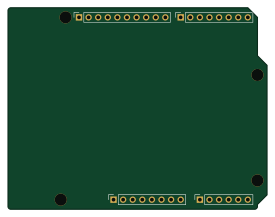
Projjet is an open source PCB design by PlanBRandom, published on GitHub under the MIT license. It is a 2-layer board measuring 68.6 × 53.3 mm, with 4 components from 4 distinct parts.
From the project
Production-grade cable harness tester using SparkFun Artemis ATP for P3/P1/P2 assemblies with automated continuity, resistance, leakage, and zener tests
Production-grade 21-channel cable harness tester for SparkFun Artemis ATP fixtures.
- Auto-generated 21x21 connectivity matrix from a simple netlist - Open, short, and crosstalk detection - Per-channel resistance measurement with JSON output - Profile-based limits for automated pass/fail checks - Python CLI, live dashboard, and CSV viewer tools
1. Open firmware/harnesstester.ino in Arduino IDE, or build from platformio.ini. 2. Install SparkFun Artemis board support. 3. Flash the firmware to the Artemis ATP. 4. Open a serial terminal at 115200` baud.
Projjet bill of materials (BOM)
4 components, 4 distinct parts.
| Qty | Part | Footprint | Refs |
|---|---|---|---|
| 1 | Power | PinSocket_1x08_P2.54mm_Vertical | J1 |
| 1 | Digital/PWM | PinSocket_1x10_P2.54mm_Vertical | J2 |
| 1 | Analog | PinSocket_1x06_P2.54mm_Vertical | J3 |
| 1 | Digital/PWM | PinSocket_1x08_P2.54mm_Vertical | J4 |
Projjet design files
The KiCad project lives in the PlanBRandom/artemis-harness-tester repository on GitHub; these links point at the commit this page was built from.
- Layoutprojjet/projjet.kicad_pcb
- Schematicprojjet/projjet.kicad_sch
Projjet: common questions
How big is the Projjet PCB?
The Projjet measures 68.6 × 53.3 mm, has 2 copper layers and is 1.6 mm thick.
How many components are on the Projjet?
4 components, from 4 distinct parts. The full bill of materials is listed on this page.
Where can I download the Projjet design files?
From the PlanBRandom/artemis-harness-tester repository on GitHub, which has the KiCad layout and the schematic; the links under Design files point to each one.
Can I use the Projjet design in my own project?
Yes, under the terms of its MIT license, which PlanBRandom chose for the repository.