Wall puzzle adapter

About the Wall puzzle adapter PCB
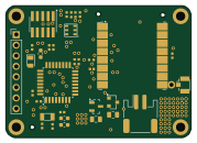
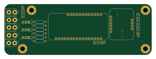
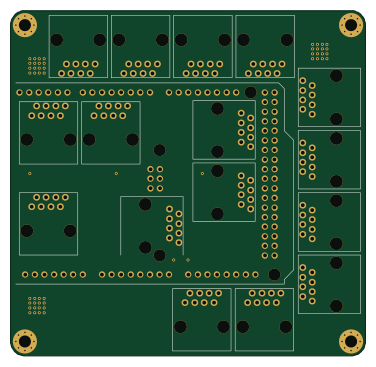
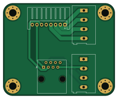
Wall puzzle adapter is an open source PCB design by rjacoby00, published on GitHub. It is a 2-layer board measuring 59.7 × 49.5 mm, with 4 components from 3 distinct parts.
From the project
Repository for code experiments and smaller projects.
This is a repository full of random bits of code I have written for various assingments, projects, and classes over time. Some of the code I am not allowed to share and has been omited due to it being private, a homework solution, copyrighted code that I cannot distribute, or secret/classified information. If you have any questions or need to see something that you think might have been redacted, feel free to email me at rjacoby00@icloud.com.
Wall puzzle adapter bill of materials (BOM)
4 components, 3 distinct parts — part numbers from the project's BOM.
| Qty | Part | Footprint | Refs |
|---|---|---|---|
| 1 | Conn_01x08_Male | RJ45_Amphenol_54602-x08_Horizontal | J1 |
| 1 | Conn_01x08_Male | JST_XH_S8B-XH-A_1x08_P2.50mm_Horizontal | J2 |
| 2 | Conn_01x04_Male | TerminalBlock_Altech_AK300-4_P5.00mm | J3, J4 |
Wall puzzle adapter design files
The KiCad project lives in the rjacoby00/devel repository on GitHub; these links point at the commit this page was built from.
Wall puzzle adapter: common questions
How big is the Wall puzzle adapter PCB?
The Wall puzzle adapter measures 59.7 × 49.5 mm, has 2 copper layers and is 1.6 mm thick.
How many components are on the Wall puzzle adapter?
4 components, from 3 distinct parts, with part numbers taken from the project's own BOM. The full bill of materials is listed on this page.
Where can I download the Wall puzzle adapter design files?
From the rjacoby00/devel repository on GitHub, which has the KiCad layout and the BOM; the links under Design files point to each one.
Can I use the Wall puzzle adapter design in my own project?
The repository has no license, so all rights stay with rjacoby00. Use it as a reference, and ask the author before reusing the design.