
Hackpad

About the Hackpad PCB
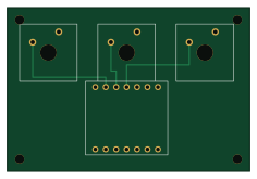
Hackpad is an open source PCB design by SiriusW823, published on GitHub under the MIT license. It is a 2-layer board measuring 59 × 40 mm, with 4 components from 2 distinct parts.
Other key parts include the XIAO. By type, the board carries 3 switches and 1 IC.
From the project
- hackpad.kicadpro - hackpad.kicadsch - hackpad.kicadpcb`
- hackpad.kicadpro - hackpad.kicadsch - hackpad.kicadpcb`
Design rules for the Hackpad submission: - Through-hole Seeed XIAO RP2040 as the MCU - PCB ≤ 100 × 100 mm - 2 layers only - Approved parts only
Gerbers exported for manufacturing go in ../production/gerbers.zip (not here).
Design constraints (for reference): through-hole XIAO RP2040, ≤100×100 mm, 2 layers.
Main components on the Hackpad
Hackpad bill of materials (BOM)
4 components, 2 distinct parts.
| Qty | Part | Footprint | Refs |
|---|---|---|---|
| 1 | XIAO | XIAO-14P-H | U1 |
| 3 | SW | SW_MX_PM | SW1, SW2, SW3 |
Hackpad design files
The KiCad project lives in the SiriusW823/Hackpad repository on GitHub; these links point at the commit this page was built from.
- LayoutPCB/hackpad.kicad_pcb
- SchematicPCB/hackpad.kicad_sch
Hackpad: common questions
How big is the Hackpad PCB?
The Hackpad measures 59 × 40 mm, has 2 copper layers and is 1.6 mm thick.
How many components are on the Hackpad?
4 components, from 2 distinct parts. The full bill of materials is listed on this page.
Where can I download the Hackpad design files?
From the SiriusW823/Hackpad repository on GitHub, which has the KiCad layout and the schematic; the links under Design files point to each one.
Can I use the Hackpad design in my own project?
Yes, under the terms of its MIT license, which SiriusW823 chose for the repository.