
Sb eps

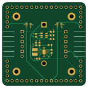
About the Sb eps PCB
Sb eps is an open source PCB design by starbelt, published on GitHub under the CC-BY-SA-4.0 license. It is a 4-layer board measuring 43 × 43 mm, with 28 components from 16 distinct parts.
Other key parts include the TPS63000IDRCRQ1, TPS3806I33QDBVRQ1 and MIC94072YC6-TR. By type, the board carries 13 connectors, 6 resistors, 4 ICs, 4 capacitors and 1 inductor.
From the project
Electrical power system (EPS) printed circuit board (PCB)
sb-eps.pretty: Footprint directory fp-lib-table: Footprint library table sb-eps.kicadpcb: KiCad PCB layout sb-eps.kicadprl: KiCad project preferences sb-eps.kicadpro: KiCad project file sb-eps.kicadsch: KiCad schematic layout sb-eps.kicadsym: KiCad symbol library sym-lib-table: Symbol library table README.md: This document
Main components on the Sb eps
Sb eps bill of materials (BOM)
28 components, 16 distinct parts — part numbers from the project's BOM.
| Qty | Part | Footprint | Refs |
|---|---|---|---|
| 1 | TPS63000IDRCRQ1 | TPS63000IDRCRQ1 | IC1 |
| 1 | TPS3806I33QDBVRQ1 | SOT95P280X145-6N | IC2 |
| 2 | MIC94072YC6-TR | SOT65P210X110-6N | IC3, IC4 |
| 3 | TSW-102-08-L-S-RA | L_HDRRA2W64P254_1X2_508X254X309P | J1, J2, J3 |
| 3 | TSW-102-08-L-S-RA | R_HDRRA2W64P254_1X2_508X254X309P | J4, J5, J6 |
| 1 | Conn_01x04 | SB_Stack_Mounting_Holes | J7 |
| 2 | CES-116-01-G-S | CES-116-XX-Y-S | J8, J9 |
| 4 | CES-104-01-G-S | CES-104-XX-Y-S | J10, J11, J12, J13 |
| 1 | SRP3212A-3R3M | INDC3225X120N | L1 |
| 1 | FT0H565ZF | FT0H565ZF | C1 |
| 3 | KAM15CT70J106KT | CAPC1608X100N | C2, C3, C4 |
| 2 | CRCW06031M15FKEA | RESC1608X50N | R1, R6 |
| 1 | CRCW0603200KFKEA | RESC1608X50N | R2 |
| 1 | CRCW0603357KFKEA | RESC1608X50N | R3 |
| 1 | CRCW0603340KFKEA | RESC1608X50N | R4 |
| 1 | CRCW0603309KFKEA | RESC1608X50N | R5 |
Sb eps design files
The KiCad project lives in the starbelt/sb-eps repository on GitHub; these links point at the commit this page was built from.
- Layoutkicad/sb-eps.kicad_pcb
- Schematickicad/sb-eps.kicad_sch
- BOMBOM.csv
Sb eps: common questions
How big is the Sb eps PCB?
The Sb eps measures 43 × 43 mm, has 4 copper layers and is 1.5422 mm thick.
How many components are on the Sb eps?
28 components, from 16 distinct parts, with part numbers taken from the project's own BOM. The full bill of materials is listed on this page.
Where can I download the Sb eps design files?
From the starbelt/sb-eps repository on GitHub, which has the KiCad layout, the schematic and the BOM; the links under Design files point to each one.
Can I use the Sb eps design in my own project?
Yes, under the terms of its CC-BY-SA-4.0 license, which starbelt chose for the repository.