
WiFiflex

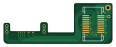
About the WiFiflex PCB
WiFiflex is an open source PCB design by supertazon, published on GitHub under the SHL-2.1 license. It is a 2-layer board measuring 28.8 × 10.5 mm, with 1 components from 1 distinct parts.
It belongs with the iot & wireless designs in this gallery.
From the project
Wii WiFi relocation flex pcb
A flex pcb to easily relocate the Wii WiFi chip for Wii portables (useless for stock Wii) by using the WiFi chip connector. The WiFi chip is notorious for being difficult to relocate by handwiring it due to wire length sensitivity. License is permissive, you are free to make, sell and distribute the flex pcb.
The flex pcb is compatible with a OMGWTF trim, it also does not overlap with the NAND relocation flex.
WiFiflex bill of materials (BOM)
1 components, 1 distinct parts.
| Qty | Part | Footprint | Refs |
|---|---|---|---|
| 1 | Conn_01x20_Pin | Molex_SlimStack_52991-0208_2x10_P0.50mm_Vertical | J1 |
WiFiflex design files
The KiCad project lives in the supertazon/WiFiflex repository on GitHub; these links point at the commit this page was built from.
WiFiflex: common questions
How big is the WiFiflex PCB?
The WiFiflex measures 28.8 × 10.5 mm, has 2 copper layers and is 0.13 mm thick.
How many components are on the WiFiflex?
1 components, from 1 distinct parts. The full bill of materials is listed on this page.
Where can I download the WiFiflex design files?
From the supertazon/WiFiflex repository on GitHub, which has the KiCad layout and the schematic; the links under Design files point to each one.
Can I use the WiFiflex design in my own project?
It is published under SHL-2.1, which limits how it may be reused; read the license before building on it.
Similar boards

RPi RM0 WiFi/Bluetooth Module
schlae
11.1 × 14 mm76 parts6LNo license1.0k
L0 IMU MPU9250
Luos-io
20.3 × 15.2 mm7 parts2LMIT547
L0 USBA
20.3 × 15.3 mm19 parts2LMIT547
L0 Controller motor
20.3 × 15.3 mm11 parts2LMIT547
L0 Dynamixel
20.3 × 15.2 mm15 parts2LMIT547
L0 stepper driver
20.3 × 15.2 mm18 parts2LMIT547