
Topplate

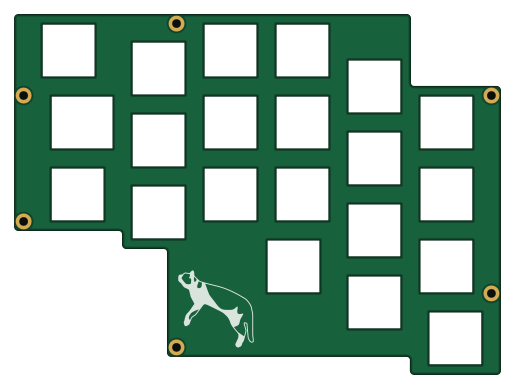
About the Topplate PCB
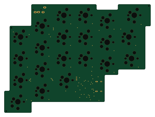
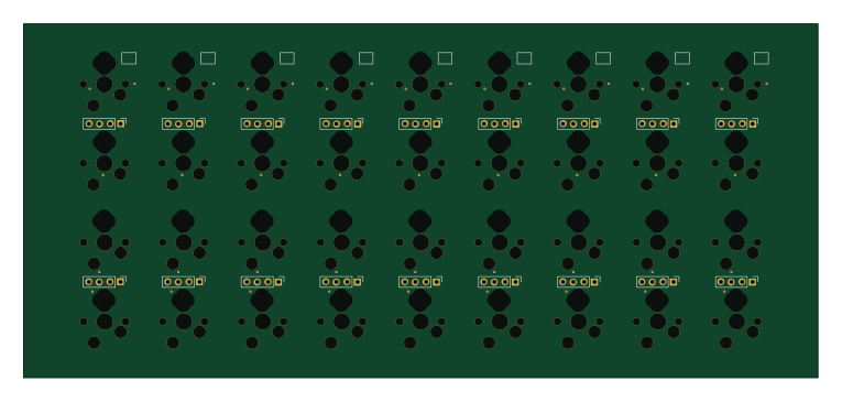
Topplate is an open source PCB design by tamaroh, published on GitHub. It is a 2-layer board measuring 128.6 × 95.3 mm, with 21 components from 2 distinct parts.
It belongs with the keyboards designs in this gallery.
From the project
- はんだ付け工具 - こて、こて台、こて先クリーナー、はんだ線など - 精密ドライバー
- はんだ付け工具 - こて、こて台、こて先クリーナー、はんだ線など - 精密ドライバー
- ピンセット - キースイッチプラー - キーキャッププラー - はんだ吸い取り線または吸い取り器 - 絶縁耐熱テープ - ## 製作手順
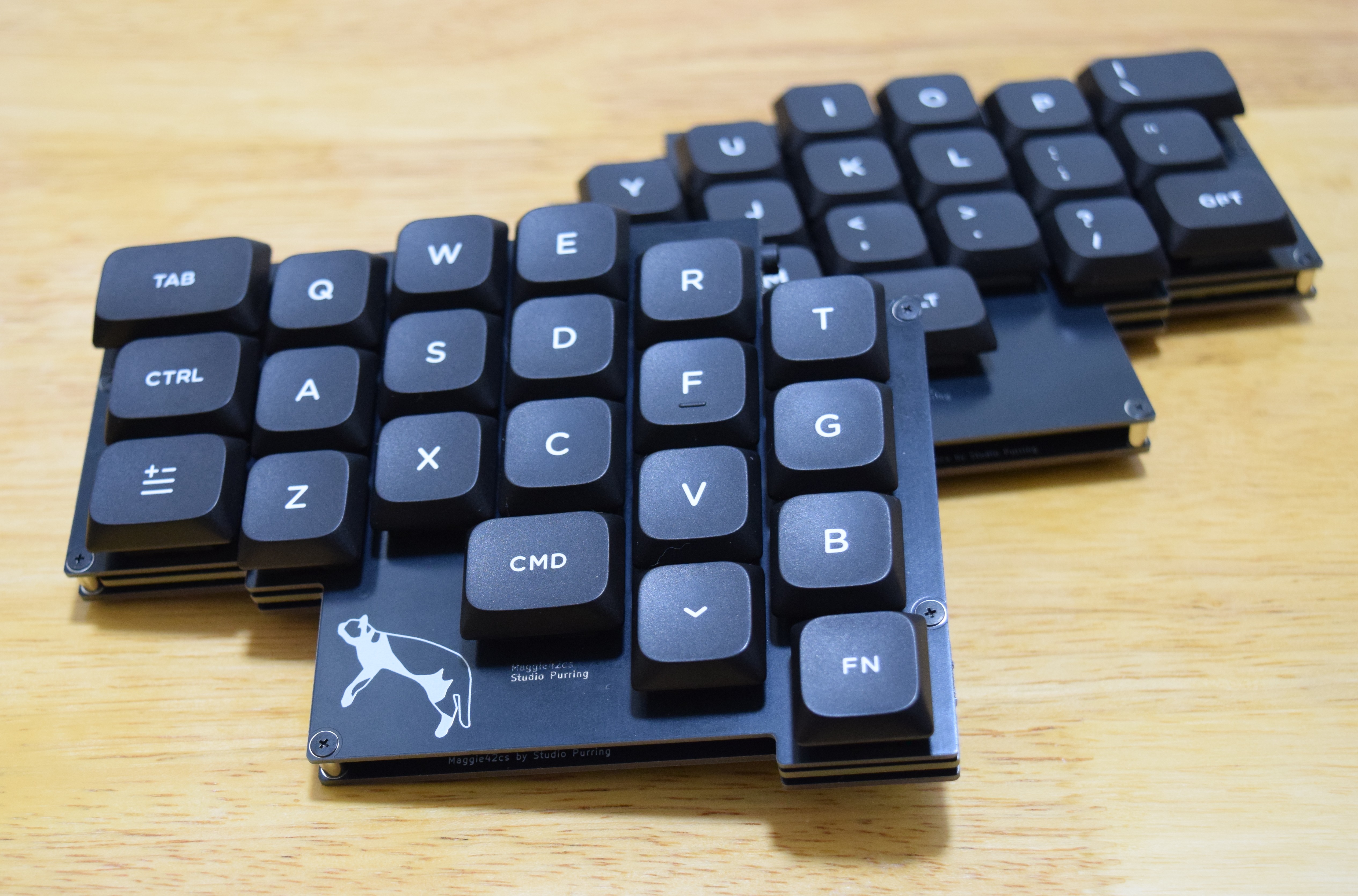
1. PCBのサポート部分を折り取ります。折った部分のデコボコが気になる場合はやすりなどで削ってください。 1. ソケットをはんだ付けします。 MXスイッチ用のソケットは上側、Chocスイッチ用のソケットは下側に設置します。 印刷に合わせて、スイッチの穴を塞がないようにします。 1. TRSコネクターをはんだ付けします。 ずれやすいのでテープなどで固定してください。 1. ファームウェアのファイル(.uf2)をダウンロードします。 https://github.com/tamaroh/maggie42cs/releases/tag/V2.0.2 1. (片側ずつ両方とも)USBケーブルを接続して、以下のいずれかの方法で RPI-RP2 リムーバブルドライブをマウントさせます。 1. BOOTSELボタンを押しながら、USBケーブルを接続します。 1. USBケーブルを接続してから、BOOTSELボタンを押しながらRESETボタンを押します。 1. 左側はTABキー、右側はYキーを押したままUSBケーブルを接続します(キースイッチ装着済みの場合)。…
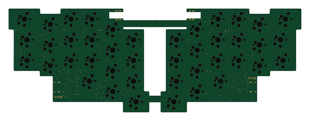
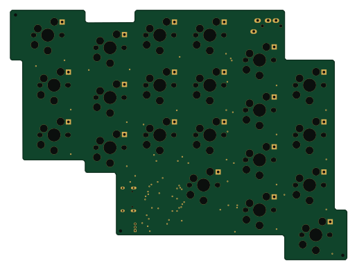
Topplate bill of materials (BOM)
21 components, 2 distinct parts.
| Qty | Part | Footprint | Refs |
|---|---|---|---|
| 20 | SW_PUSH | SW_Hole | SW1, SW2, SW3, SW4, SW5, SW6, SW8, SW9 +12 |
| 1 | SW_PUSH | SW_Hole_1+1.25 | SW7 |
Topplate design files
The KiCad project lives in the tamaroh/maggie42cs repository on GitHub; these links point at the commit this page was built from.
- Layoutpcb/topplate.kicad_pcb
Topplate: common questions
How big is the Topplate PCB?
The Topplate measures 128.6 × 95.3 mm, has 2 copper layers and is 1.6 mm thick.
How many components are on the Topplate?
21 components, from 2 distinct parts. The full bill of materials is listed on this page.
Where can I download the Topplate design files?
From the tamaroh/maggie42cs repository on GitHub, which has the KiCad layout; the links under Design files point to each one.
Can I use the Topplate design in my own project?
The repository has no license, so all rights stay with tamaroh. Use it as a reference, and ask the author before reusing the design.
 byrantech

 google