
Laser Backplane DVI

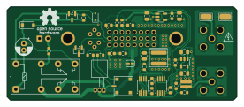
About the Laser Backplane DVI PCB
Laser Backplane DVI is an open source PCB design by TU-Darmstadt-APQ, published on GitHub under the CERN-OHL-W-2.0 license. It is a 2-layer board measuring 69 × 28 mm, with 41 components from 30 distinct parts.
Other key parts include the ADA4807-2ARMZ, LT1761IS5-5#TRPBF, LT1964IS5-5#TRPBF and AT21CS11-STU10-T. By type, the board carries 14 capacitors, 10 resistors, 4 ICs, 4 connectors, 3 diodes and 3 inductors.
From the project
Laser backplane with DVI connector featuring fast current modulation and a laser diode protection.
Note on the compliance voltage The compliance voltage of the Howland Current Pump is half of the positive output voltage swing of the operational amplifier. The circuit is implemented by a rail-to-rail output operational amplifier (ADA4807) supplied by ±5 V. Hence, the voltage at the laser diode anode is limited to 2.4 V accounting for a small head-room. Some additional head-room should be reserved for the (small) rise of the voltage required for the maximal output of the current source (5 mA). The maximal laser diode anode voltage is sufficient as a compliance voltage for infra red laser…
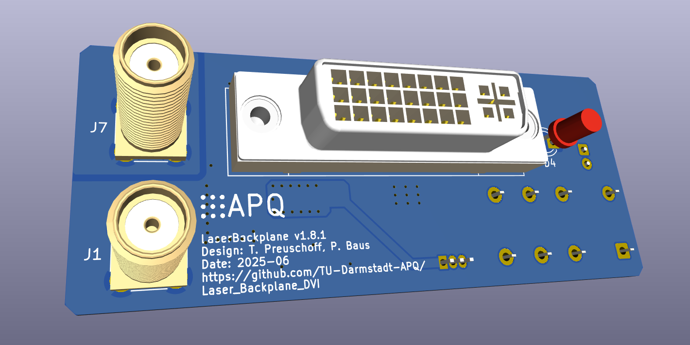
Main components on the Laser Backplane DVI
Laser Backplane DVI bill of materials (BOM)
41 components, 30 distinct parts.
| Qty | Part | Footprint | Refs |
|---|---|---|---|
| 1 | ADA4807-2ARMZ ADA4807-2ARM | MSOP-8_3x3mm_P0.65mm | U1 |
| 1 | LT1761IS5-5#TRPBF LT1761-5 | TSOT-23-5 | U2 |
| 1 | LT1964IS5-5#TRPBF LT1964-5 | TSOT-23-5 | U3 |
| 1 | AT21CS11-STU10-T | SOT-23 | U4 |
| 1 | MMBT3904-QR MMBT3904 | SOT-23 | Q1 |
| 1 | 2N4401BU 2N4401 | TO-92_Inline_Horizontal1 | Q2 |
| 1 | 132291 Curr. Mod. | SMA_Amphenol_132291_Vertical | J1 |
| 1 | CDVI-F29VDG1-P1 DVI-I | DVI-I_Conn-Link_CDVI-F29VDG1-P1_Vertical | J2 |
| 1 | 132291 Piezo_In | SMA_Amphenol_132291_Vertical | J7 |
| 1 | CONSMP001-SMD-G-T Conn_Coaxial | SMP_TE_CONSMP001-SMD-G-T_Vertical | J8 |
| 1 | G6AU-274P-ST-US DC9 G6AU | Relay_DPDT_Omron_G6A | K1 |
| 1 | BAS21GWX | D_SOD-123 | D1 |
| 1 | BAS3010B03WE6327HTSA1 BAS3010B | D_SOD-323 | D2 |
| 1 | WP424GDT Green | LED_D3.0mm_FlatTop | D4 |
| 2 | BLM18KG102SZ1D | L_0603_1608Metric | FB1, FB2 |
| 1 | XGL5050-333MEC 33u | Coilcraft_XGL5050 | L1 |
| 4 | CGA3E2C0G1H103J080AE 10n | C_0603_1608Metric | C1, C6, C8, C11 |
| 1 | CGA3E2X7R1H103K080AA 10n | C_0603_1608Metric | C2 |
| 1 | 860040572002 47u | CP_Radial_D5.0mm_P2.00mm | C3 |
| 1 | C0603C159C5GACAUTO 1.5p | C_0603_1608Metric | C4 |
Show 10 more
| Qty | Part | Footprint | Refs |
|---|---|---|---|
| 1 | DNF | C_0603_1608Metric | C5 |
| 4 | CGA4J1X7R1V475K125AC 4.7u | C_0805_2012Metric | C7, C9, C10, C12 |
| 2 | C0603C104K5RACAUTO 100n | C_0603_1608Metric | C13, C14 |
| 1 | RG2012P-49R9-D-T5 49.9R | R_0805_2012Metric | R1 |
| 1 | LTR18EZPF49R9 49.9R | R_0612_1632Metric | R2 |
| 1 | CRCW060347K0FKEA 47k | R_0603_1608Metric | R3 |
| 1 | RG1608Q-100-D-T5 10R | R_0603_1608Metric | R4 |
| 4 | RG1608P-102-D-T5 1k | R_0603_1608Metric | R5, R6, R7, R8 |
| 1 | RNCP0603FTD4R70 4.7R | R_0603_1608Metric | R9 |
| 1 | MORNTA1001AT5 1k | MSOP-8_3x3mm_P0.65mm | RN1 |
Laser Backplane DVI design files
The KiCad project lives in the TU-Darmstadt-APQ/Laser_Backplane_DVI repository on GitHub; these links point at the commit this page was built from.
Laser Backplane DVI: common questions
How big is the Laser Backplane DVI PCB?
The Laser Backplane DVI measures 69 × 28 mm, has 2 copper layers and is 1.6 mm thick.
How many components are on the Laser Backplane DVI?
41 components, from 30 distinct parts. The full bill of materials is listed on this page.
Where can I download the Laser Backplane DVI design files?
From the TU-Darmstadt-APQ/Laser_Backplane_DVI repository on GitHub, which has the KiCad layout and the schematic; the links under Design files point to each one.
Can I use the Laser Backplane DVI design in my own project?
Yes, under the terms of its CERN-OHL-W-2.0 license, which TU-Darmstadt-APQ chose for the repository.