
Ai pcb

About the Ai pcb
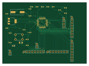
Ai pcb is an open source STM32 PCB design by 123Nert, published on GitHub. It is a 2-layer board measuring 78 × 57 mm, with 31 components from 21 distinct parts.
Its main chip is the STM32F103C8T6, from the STM32 family. Other key parts include the AMS1117-3.3. By type, the board carries 14 capacitors, 7 connectors, 3 resistors, 2 ICs, 2 crystals and 1 switch.
From the project
AI+Kicad
1. 用 ST-Link 连接 J1:SWDIO → SWDIO,SWCLK → SWCLK,GND → GND,3V3 → 3V3 2. BOOT0 已下拉,上电即从 Flash 启动,直接可在 STM32CubeProgrammer / Keil / OpenOCD 中下载调试 3. 串口下载(可选):USB-TTL 接 PA9(TX) / PA10(RX),BOOT0 排针接 3V3 后复位进入系统bootloader
- 板框:78 × 57 mm,双层板(F.Cu 信号 / B.Cu 整面 GND 铺铜) - 线宽:信号 0.15–0.25 mm,电源 0.5 mm - 过孔:0.6/0.3 mm(外径/钻孔) - 最小线宽约束:0.1 mm(嘉立创等板厂均可制造)
1. 原理图:通过 MCP 工具(kicad-sch-api)放置器件、连线、标注网络 2. 封装:全部器件指定 KiCad 标准封装(0603 阻容 / LQFP-48 / SOT-223 / 2.54mm 排针) 3. PCB:脚本创建板框与布局,按网表分配焊盘网络 4. 布线:导出 Specctra DSN → Freerouting 自动布线(94 网络全通)→ 导入 SES 5. 验证:ERC / DRC 全部通过(剩余仅丝印外观类提示)
Main components on the Ai pcb
Ai pcb bill of materials (BOM)
31 components, 21 distinct parts.
| Qty | Part | Footprint | Refs |
|---|---|---|---|
| 1 | STM32F103C8T6 | LQFP-48_7x7mm_P0.5mm | U1 |
| 1 | AMS1117-3.3 | SOT-223-3_TabPin2 | U2 |
| 1 | 8MHz | Crystal_SMD_HC49-SD | Y1 |
| 1 | 32.768kHz | Crystal_SMD_3215-2Pin_3.2x1.5mm | Y2 |
| 1 | SWD | PinHeader_1x04_P2.54mm_Vertical | J1 |
| 1 | PA0-PA7 | PinHeader_1x08_P2.54mm_Vertical | J2 |
| 1 | PA8-PA15 | PinHeader_1x08_P2.54mm_Vertical | J3 |
| 1 | PB0-PB7 | PinHeader_1x08_P2.54mm_Vertical | J4 |
| 1 | PB8-PB15 | PinHeader_1x08_P2.54mm_Vertical | J5 |
| 1 | PC13/NRST | PinHeader_1x02_P2.54mm_Vertical | J6 |
| 1 | 5V_IN | PinHeader_1x02_P2.54mm_Vertical | J7 |
| 1 | RESET | SW_PUSH_6mm | SW1 |
| 1 | PWR | LED_0603_1608Metric | LED1 |
| 1 | 600R@100MHz | L_0603_1608Metric | FB1 |
| 2 | 20pF | C_0603_1608Metric | C1, C2 |
| 6 | 100nF | C_0603_1608Metric | C3, C4, C5, C6, C8, C10 |
| 3 | 10uF | C_0603_1608Metric | C7, C13, C14 |
| 1 | 1uF | C_0603_1608Metric | C9 |
| 2 | 12pF | C_0603_1608Metric | C11, C12 |
| 2 | 10k | R_0603_1608Metric | R1, R2 |
Show 1 more
| Qty | Part | Footprint | Refs |
|---|---|---|---|
| 1 | 1k | R_0603_1608Metric | R3 |
Ai pcb design files
The KiCad project lives in the 123Nert/ai_pcb repository on GitHub; these links point at the commit this page was built from.
- Layoutstm32f103_min_sys.kicad_pcb
- Schematicstm32f103_min_sys.kicad_sch
Ai pcb: common questions
What microcontroller does the Ai pcb use?
The Ai pcb is built around the STM32F103C8T6, from the STM32 family.
How big is the Ai pcb?
The Ai pcb measures 78 × 57 mm, has 2 copper layers and is 1.6 mm thick.
How many components are on the Ai pcb?
31 components, from 21 distinct parts. The full bill of materials is listed on this page.
Where can I download the Ai pcb design files?
From the 123Nert/ai_pcb repository on GitHub, which has the KiCad layout and the schematic; the links under Design files point to each one.
Can I use the Ai pcb design in my own project?
The repository has no license, so all rights stay with 123Nert. Use it as a reference, and ask the author before reusing the design.
Can I test firmware for the Ai pcb without the hardware?
Yes. HardLabs builds a simulation of the board from its netlist and BOM, so you can run and debug STM32 firmware against it before you order a PCB.
Similar boards
 STM32
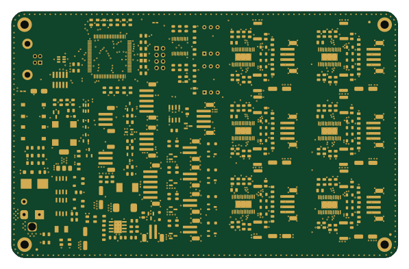
STM32LumenPnP Motherboard
opulo-inc
149 × 95 mm296 parts4LCC-BY-SA-4.03.7k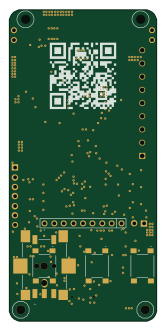 STM32
STM32AxxSolder
AxxAxx
39 × 82.5 mm122 parts2LGPL-3.01.7k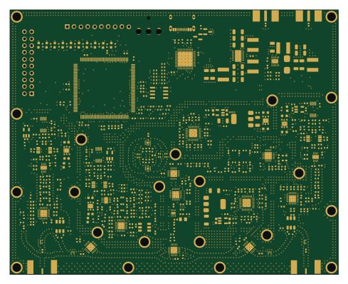 STM32
STM32LibreVNA
jankae
122 × 98 mm592 parts6LGPL-3.01.6k STM32
STM32AIOC
skuep
21 × 31.5 mm47 parts2LMIT1.4k STM32
STM32Ferris
pierrechevalier83
208.8 × 86.8 mm102 parts2LSHL-2.11.3k STM32
STM32176 pin board
rusefi
61.8 × 73.2 mm76 parts2LGPL-3.01.2k