
Sd net-2.0

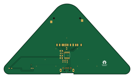
About the Sd net-2.0 PCB
Sd net-2.0 is an open source PCB design by 1phonetucked-tech, published on GitHub under the CERN-OHL-S-2.0 license. It is a 4-layer board measuring 117 × 65 mm, with 13 components from 7 distinct parts.
Other key parts include the GL823K-HCY04. By type, the board carries 8 capacitors, 1 IC, 1 LED and 1 resistor.
From the project
Open-source full-size USB SD card reader (GL823K). CERN-OHL-S-2.0.
full-size USB SD card reader > USB-A plug for end user connect > 13 placements across 7 line items in between.
hardware, everything in hardware/ and fab/ > CERN-OHL-S-2.0 > distribute a variant and its design files must be shared under the same terms documentation, everything in docs/ > CC-BY-SA-4.0 > credit the source, share adaptations alike software, the generators in tools/ > GPL-3.0 > see tools/LICENSE
Main components on the Sd net-2.0
Sd net-2.0 bill of materials (BOM)
13 components, 7 distinct parts — part numbers from the project's BOM.
| Qty | Part | Footprint | Refs |
|---|---|---|---|
| 1 | GL823K-HCY04 Genesys Logic | SSOP-16_3.9x4.9mm_P0.635mm | U1 |
| 1 | SD-006M Sofng | SD-006M | CARD1 |
| 1 | AM90 Shou Han | USB-AM90 | USB1 |
| 1 | 12-215SYGC/S530-E2/TR8 12-215SYGC Everlight | LED-12-215SYGC | LED1 |
| 3 | CL21A106KAYNNNE 10uF Samsung | C_0805_2012Metric | C1, C2, C3 |
| 5 | CC0603KRX7R9BB104 100nF Yageo | C_0603_1608Metric | C4, C5, C6, C7, C8 |
| 1 | 0603WAF2200T5E 220 Uni-Royal | R_0603_1608Metric | R1 |
Sd net-2.0 design files
The KiCad project lives in the 1phonetucked-tech/sd-net-2.0 repository on GitHub; these links point at the commit this page was built from.
Sd net-2.0: common questions
How big is the Sd net-2.0 PCB?
The Sd net-2.0 measures 117 × 65 mm, has 4 copper layers and is 1.6 mm thick.
How many components are on the Sd net-2.0?
13 components, from 7 distinct parts, with part numbers taken from the project's own BOM. The full bill of materials is listed on this page.
Where can I download the Sd net-2.0 design files?
From the 1phonetucked-tech/sd-net-2.0 repository on GitHub, which has the KiCad layout, the schematic and the BOM; the links under Design files point to each one.
Can I use the Sd net-2.0 design in my own project?
Yes, under the terms of its CERN-OHL-S-2.0 license, which 1phonetucked-tech chose for the repository.