
SKA40

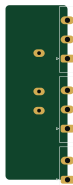
About the SKA40 PCB
SKA40 is an open source PCB design by AbdELRahmanGamiel, published on GitHub. It is a 2-layer board measuring 16.4 × 46.2 mm, with 4 components from 4 distinct parts.
Other key parts include the L7805. By type, the board carries 3 connectors and 1 IC.
Main components on the SKA40
SKA40 bill of materials (BOM)
4 components, 4 distinct parts — part numbers from the project's BOM.
| Qty | Part | Footprint | Refs |
|---|---|---|---|
| 1 | L7805 SKA40 | SKA40 | U1 |
| 1 | INPUT | PhoenixContact_MSTBA_2,5_3-G-5,08_1x03_P5.08mm_Horizontal | J1 |
| 1 | 12V_INPUT RS | PhoenixContact_MSTBA_2,5_2-G-5,08_1x02_P5.08mm_Horizontal | J2 |
| 1 | OUTPUT | PhoenixContact_MSTBA_2,5_3-G-5,08_1x03_P5.08mm_Horizontal | J3 |
SKA40 design files
The KiCad project lives in the AbdELRahmanGamiel/PcbDesignsHw repository on GitHub; these links point at the commit this page was built from.
SKA40: common questions
How big is the SKA40 PCB?
The SKA40 measures 16.4 × 46.2 mm, has 2 copper layers and is 1.6 mm thick.
How many components are on the SKA40?
4 components, from 4 distinct parts, with part numbers taken from the project's own BOM. The full bill of materials is listed on this page.
Where can I download the SKA40 design files?
From the AbdELRahmanGamiel/PcbDesignsHw repository on GitHub, which has the KiCad layout and the BOM; the links under Design files point to each one.
Can I use the SKA40 design in my own project?
The repository has no license, so all rights stay with AbdELRahmanGamiel. Use it as a reference, and ask the author before reusing the design.
More boards in PcbDesignsHw
 AVR/Arduino
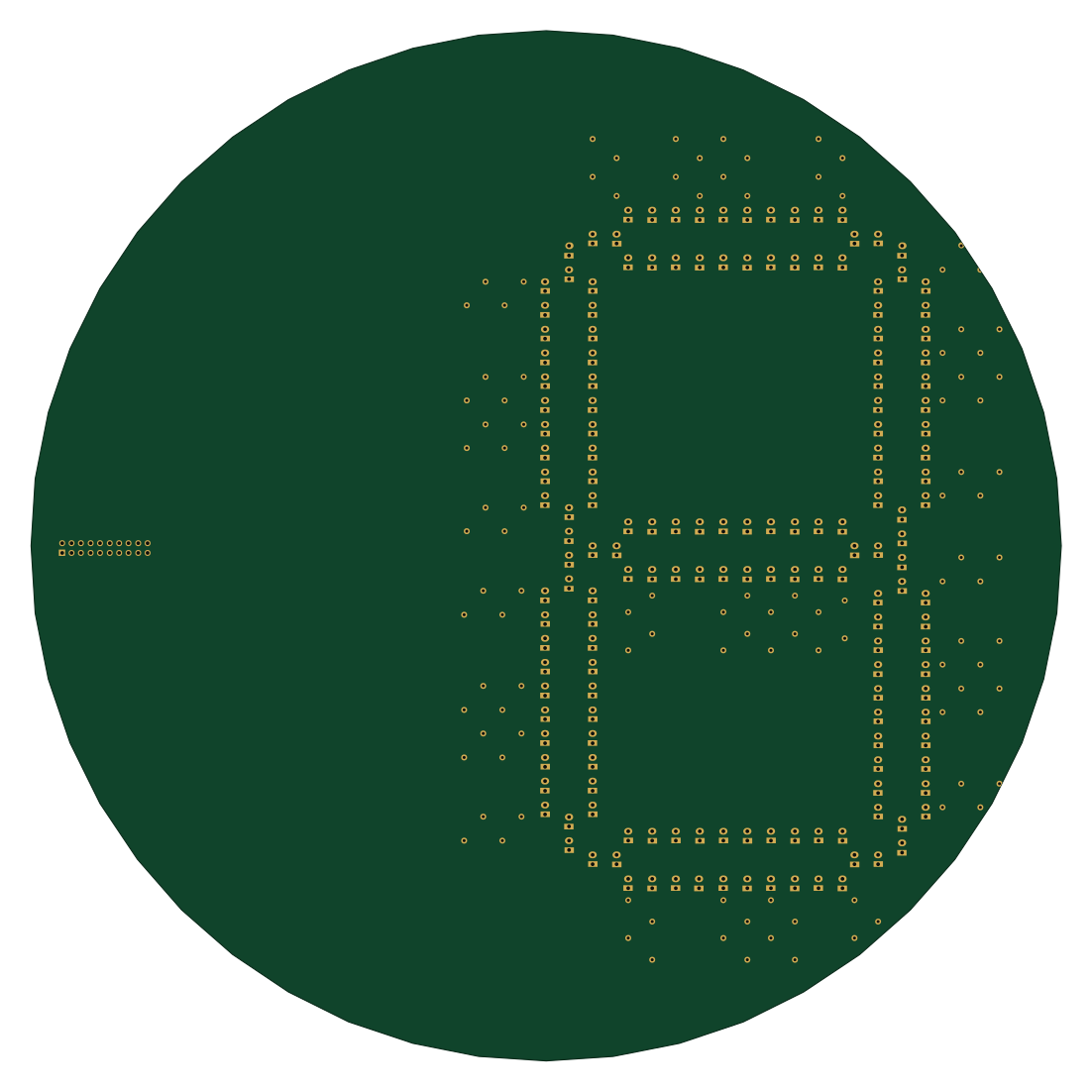
Counter sema lens30cm
275 × 275 mm585 parts2LNo license0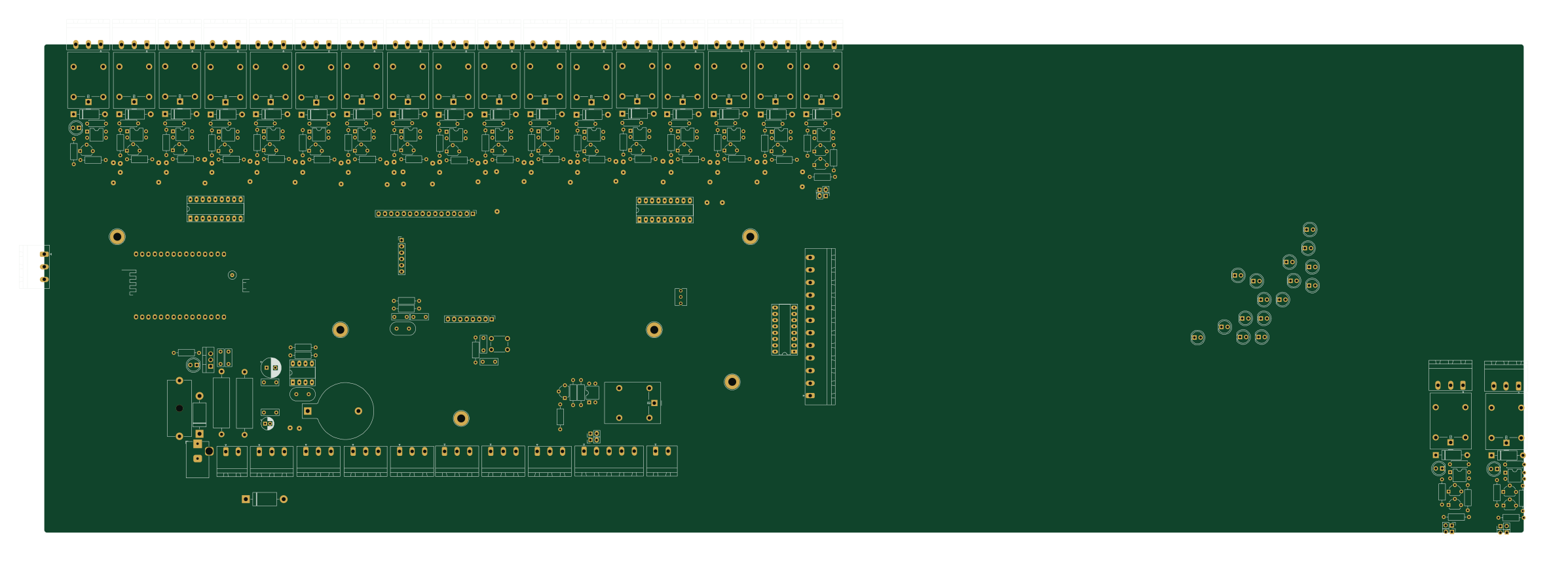 ESP32
ESP32ThePlatform MothedahFarm V2.0
597.6 × 197.2 mm243 parts2LNo license0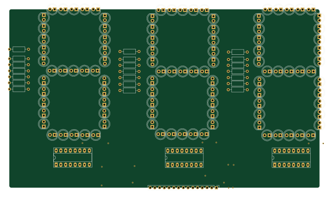 AVR/Arduino
7SEG 3
166.2 × 95.6 mm130 parts2LNo license0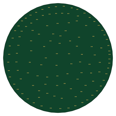
Pick&place test
100 × 100 mm120 parts2LNo license0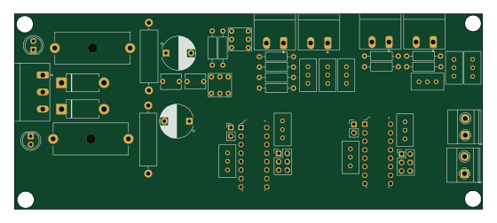
Oscilliscope channel
139.7 × 58.4 mm47 parts2LNo license0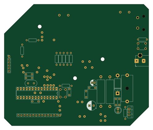 ESP8266
7SEG CONTROL V1
123.4 × 103.9 mm37 parts2LNo license0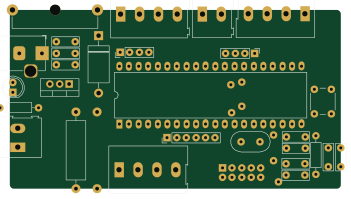 AVR/Arduino
Q
87.6 × 47.3 mm32 parts2LNo license0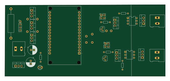 ESP32
ESP32Heater
138.1 × 62.1 mm28 parts2LNo license0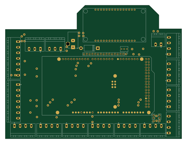 ESP8266
Future uni
159.5 × 120.8 mm23 parts2LNo license0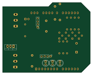 AVR/Arduino
PCB shield
74.8 × 60.1 mm23 parts2LNo license0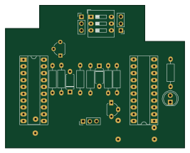
UART to SDI-12
66.6 × 53 mm18 parts2LNo license0