
SWD2USBC

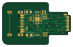
About the SWD2USBC PCB
SWD2USBC is an open source AVR/Arduino PCB design by alvarop, published on GitHub under the CC0-1.0 license. It is a 4-layer board measuring 25.8 × 16 mm, with 16 components from 13 distinct parts.
Its main chip is the ATTINY24A-MMH, from the AVR/Arduino family. By type, the board carries 8 resistors, 3 connectors, 2 diodes, 2 capacitors and 1 IC.
It belongs with the usb & debug tools designs in this gallery.
From the project
Have you ever wanted to debug your device over USB-C? Sometimes there's not enough room for a JTAG/SWD connector, or even Tag-Connect pads!
Have you ever wanted to debug your device over USB-C? Sometimes there's not enough room for a JTAG/SWD connector, or even Tag-Connect pads!
For history and all of the details, check out my detailed write up here.
Full featured adapter with Debug Accessory Mode support. Includes an ATTiny microcontroller to set the correct pull-up resistors on CC1/CC2 to provide accurate charge current to the target. Has a USB-C plug so no extra USB-C cable required
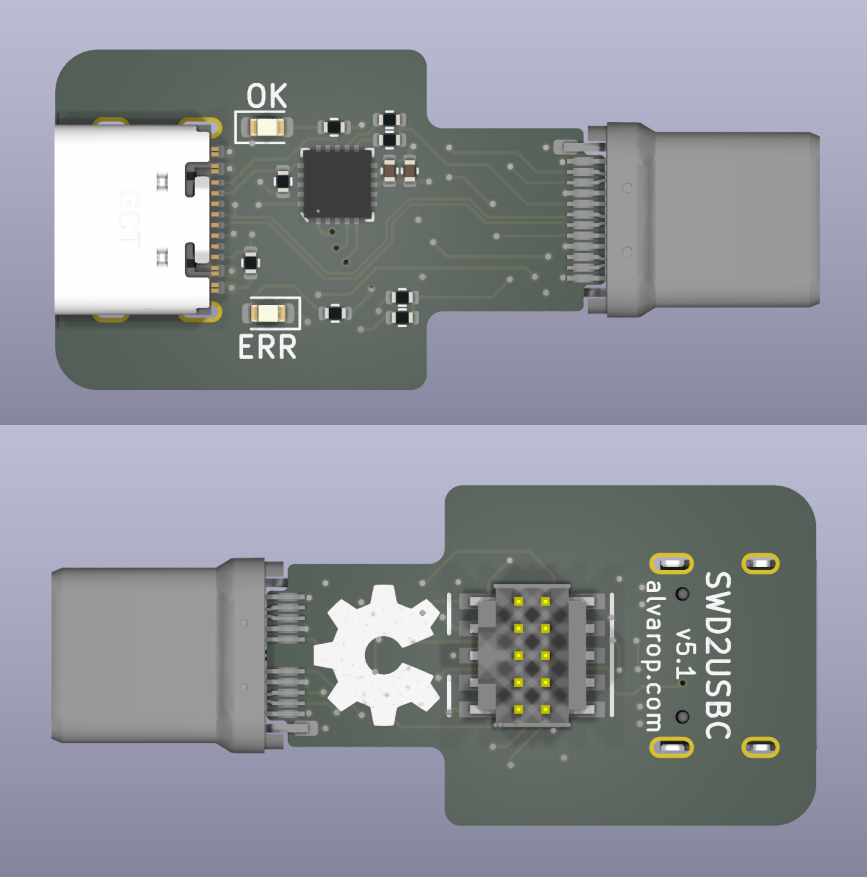
Main components on the SWD2USBC
SWD2USBC bill of materials (BOM)
16 components, 13 distinct parts.
| Qty | Part | Footprint | Refs |
|---|---|---|---|
| 1 | ATTINY24A-MMH ATtiny24-20M Microchip | ATTINY24A-MMH | U1 |
| 1 | USB4105-GF-A USB_C_Receptacle_USB2.0 GCT | USB4105-GF-A | J1 |
| 1 | FTSH-105-01-F-DV-K Conn_ARM_JTAG_SWD_10 Samtec Inc. | SAMTEC_FTSH-105-01-F-DV-P-TR | J2 |
| 1 | 1054440011 USB_C_Plug Molex | MOLEX_1054440011 | P1 |
| 1 | SML-D12M8WT86 GREEN Rohm Semiconductor | LED_0603_1608Metric | D1 |
| 1 | SML-D12U1WT86 RED Rohm Semiconductor | LED_0603_1608Metric | D2 |
| 1 | CL05A105KO5NNNC 1uF Samsung Electro-Mechanics | C_0402_1005Metric | C1 |
| 1 | CL05B104KO5NNNC 0.1uF Samsung Electro-Mechanics | C_0402_1005Metric | C2 |
| 2 | RC0402FR-075K1L 5.1k Yageo | R_0402_1005Metric | R1, R2 |
| 1 | RC0402FR-0710KL 10k Yageo | R_0402_1005Metric | R3 |
| 2 | RC0402FR-0722KL 22k Yageo | R_0402_1005Metric | R4, R5 |
| 1 | RC0402FR-0756KL 56k Yageo | R_0402_1005Metric | R6 |
| 2 | RC0402FR-071KL 1k Yageo | R_0402_1005Metric | R7, R8 |
SWD2USBC design files
The KiCad project lives in the alvarop/swd2usbc repository on GitHub; these links point at the commit this page was built from.
- Layoutswd2usbc/swd2usbc.kicad_pcb
- Schematicswd2usbc/swd2usbc.kicad_sch
SWD2USBC: common questions
What microcontroller does the SWD2USBC use?
The SWD2USBC is built around the ATTINY24A-MMH, from the AVR/Arduino family.
How big is the SWD2USBC PCB?
The SWD2USBC measures 25.8 × 16 mm, has 4 copper layers and is 0.8 mm thick.
How many components are on the SWD2USBC?
16 components, from 13 distinct parts. The full bill of materials is listed on this page.
Where can I download the SWD2USBC design files?
From the alvarop/swd2usbc repository on GitHub, which has the KiCad layout and the schematic; the links under Design files point to each one.
Can I use the SWD2USBC design in my own project?
Yes, under the terms of its CC0-1.0 license, which alvarop chose for the repository.
Can I test firmware for the SWD2USBC without the hardware?
Yes. HardLabs builds a simulation of the board from its netlist and BOM, so you can run and debug AVR/Arduino firmware against it before you order a PCB.
More boards in swd2usbc
Similar boards
 AVR/Arduino
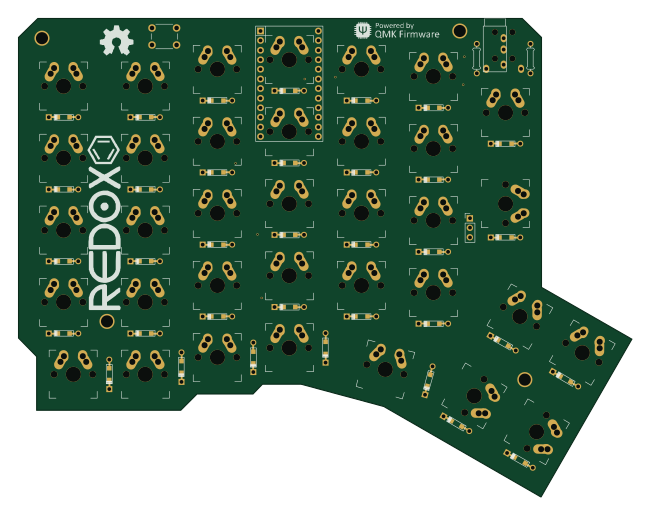
Redox keyboard
mattdibi
162.2 × 126.5 mm77 parts2LMIT2.0k AVR/Arduino
ModuleV450
stuartpittaway
30 × 61.4 mm39 parts2LCC-BY-NC-4.01.1k AVR/Arduino
V4
30 × 50 mm38 parts2LCC-BY-NC-4.01.1k AVR/Arduino
Discipline
coseyfannitutti
304.9 × 122.8 mm170 parts2LCC-BY-NC-4.01.0k AVR/Arduino
Megadesk
gcormier
41.7 × 32.2 mm23 parts2LGPL-3.0818 AVR/Arduino
Easyduino Atmega Nano
Hanqaqa
43.4 × 18 mm30 parts4LCERN-OHL-P-2.0746