
EKA-PiF-MIFA

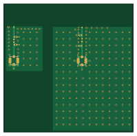
About the EKA-PiF-MIFA PCB
EKA-PiF-MIFA is an open source PCB design by Blaze-Pascal, published on GitHub under the MIT license. It is a 2-layer board measuring 49.7 × 49.3 mm, with 10 components from 5 distinct parts.
By type, the board carries 4 capacitors, 2 connectors, 2 antennas and 2 inductors.
It belongs with the iot & wireless, rf & radio and test & measurement designs in this gallery.
From the project
2.4 GHz MIFA trace antenna design and simulation. Modeled using Ansys HFSS with Optimetrics sweeps to optimize geometry. Implemented on a custom 2-layer KiCad PCB using a coplanar waveguide. Includes LiteVNA verification diagnostics and a calculated Pi impedance matching network.
Goal: Design, simulate, and measure a custom Meandered Inverted-F Antenna (MIFA) for the 2.4 GHz ISM band (Wi-Fi/Bluetooth).
Project Scope: - Literature Review: Studied reference designs and application notes from credible silicon manufacturers (TI, NXP). - RF Simulation: Modeled and optimized the antenna geometry using Ansys HFSS. - Hardware Prototyping: Exported the optimized geometry to KiCad, designed a 2-layer test PCB, and manufactured the prototype. - VNA Verification & Matching: Measured the physical antenna with a LiteVNA to verify simulation results, and designed a Pi matching…
EKA-PiF-MIFA bill of materials (BOM)
10 components, 5 distinct parts.
| Qty | Part | Footprint | Refs |
|---|---|---|---|
| 2 | Conn_Coaxial | U.FL_Molex_MCRF_73412-0110_Vertical | J101, J102 |
| 1 | TI Ref | Texas_SWRA117D_2.4GHz_Right | AE101 |
| 1 | The Stizz | Blaze_2.4GHz_MIFA | AE102 |
| 2 | 0H | L_0402_1005Metric | L101, L102 |
| 4 | DNP | C_0402_1005Metric | C101, C102, C103, C104 |
EKA-PiF-MIFA design files
The KiCad project lives in the Blaze-Pascal/EKA-PiF-MIFA repository on GitHub; these links point at the commit this page was built from.
- LayoutKiCad/AntTest.kicad_pcb
- SchematicKiCad/AntTest.kicad_sch
EKA-PiF-MIFA: common questions
How big is the EKA-PiF-MIFA PCB?
The EKA-PiF-MIFA measures 49.7 × 49.3 mm, has 2 copper layers and is 1.6 mm thick.
How many components are on the EKA-PiF-MIFA?
10 components, from 5 distinct parts. The full bill of materials is listed on this page.
Where can I download the EKA-PiF-MIFA design files?
From the Blaze-Pascal/EKA-PiF-MIFA repository on GitHub, which has the KiCad layout and the schematic; the links under Design files point to each one.
Can I use the EKA-PiF-MIFA design in my own project?
Yes, under the terms of its MIT license, which Blaze-Pascal chose for the repository.
Similar boards
StackLink
gusmanb
52.3 × 10.5 mm5 parts2LGPL-3.05.0k
AnalyzerBoxPCB fork
52.7 × 47.9 mm54 parts4LGPL-3.05.0k
LevelShifter
28.3 × 39.8 mm21 parts2LGPL-3.05.0k
RPi RM0 WiFi/Bluetooth Module
schlae
11.1 × 14 mm76 parts6LNo license1.0k
Radioberry preamp
pa3gsb
65 × 56 mm137 parts2LNo license675
Radioberry juice
65 × 56 mm87 parts2LNo license675